OCS-I/O Modules
See Also (opens another page):
Go To (remain on this page):
Topic Menu
OCS-I/O via CsCAN
Horner OCS-I/O is a Remote I/O option that connects via CsCAN Network to all Horner OCS host Controllers that includes XL series, Micro OCS series, XL Prime , and XL Canvas Series.
OCS-I/O hardware consists of a Horner HE959CNX116 CsCAN Base Unit with up to 7 Horner OCS I/O Modules stacked onto it. Controllers which have CsCAN port supports CsCAN I/O Configuration, including OCS-I/O modules.
Note:
-
Each Host Controller can access up to 16 OCS-I/O Base Units.
-
OCS-I/O is supported on the CAN1 port only (in dual CAN ports devices)
-
OCS I/O only works with a Baud Rate of 125Kb.
OCS-I/O Configuration
To configure OCS-I/O, from Hardware Configuration dialog, select the model that supports CsCAN I/O and click on the ‘CsCAN I/O’ tab.
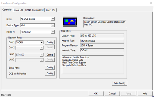
Select CAN1 (CsCAN) I/O to open the screen below:
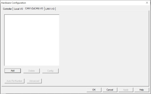
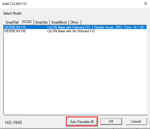
Selecting Add opens the following dialog:
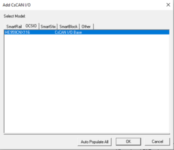
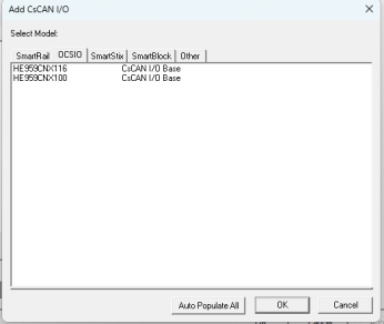
The CsCAN I/O supports Smart Rail, OCS-I/O, Smart Stix, Smart Block & other types of modules.
Selecting OCS-I/O tab brings up the below displayed window:
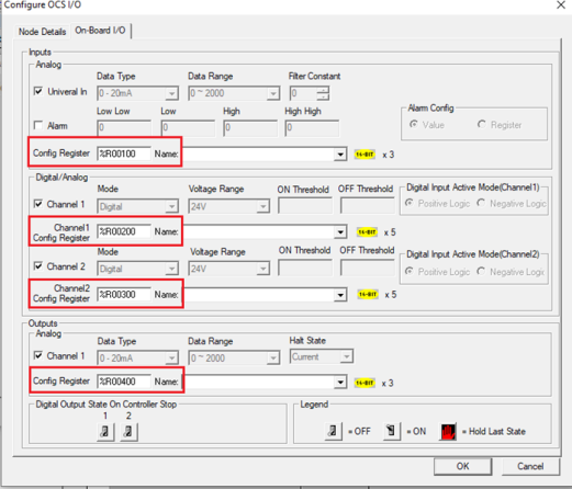
Select HE959CNX116 in the OCS-I/O tab and then click the OK button, which opens the Configure OCS-I/O dialog, as shown below:
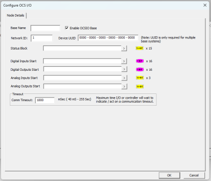
Node Details
-
Base Name: Any descriptive text (0 to 15 characters).
-
Network ID: OCS-I/O Base Unit Network ID (1 to 79). NOTE: In single OCS-I/O base configuration change in Network ID requires power cycling of the base to re-establish communication with the host controller.
-
Enable OCS-I/O: When this option is checked Input/Output data from Host controller will get transmitted to OCS-I/O. If the option is unchecked Input /Output data will NOT get transmitted to OCS-I/O but communication between the Host controller and OCS-I/O will be healthy.
-
Device UUID: Each OCS-I/O base requires a Unique ID to establish communication with the host controller. In case of Single Base OCS-I/O entering UUID is not required, host controller can automatically assign that. In case of Multiple base configurations, it is Mandatory to enter UUID of each base.
-
Status Register: Host controller reports the communication status of the OCS-I/O Base unit and stacked IO Modules in Fifteen consecutive registers
-
Digital Inputs Start: Start of OCS register block where digital input data will be stored
-
Digital Outputs Start: Start of OCS register block containing source data for digital outputs
-
Analog Inputs Start: Start of OCS register block where analog input data will be stored
-
Analog Outputs Start: Start of OCS register block containing source data for analog outputs
-
Comm Timeout: Maximum time Base Unit or Host Controller will wait to indicate / act on loss of communication (40 to 255000 mS).
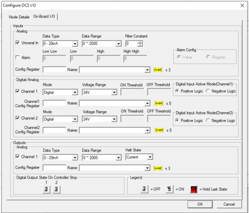
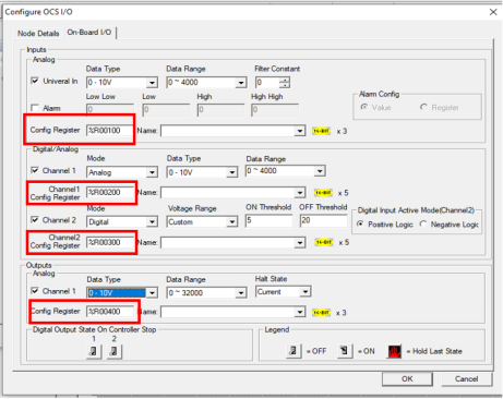
Onboard I/O
OCS-I/O base supports 2 Digital/Analog Inputs, 1 universal Analog Input and 1 Analog Output. Configuration for this Inputs/outputs are done by selecting Onboard I/O tab.
Selecting Onboard I/O displays below window:
Return to the Top: OCS-I/O Modules
OCS-I/O Base Identification
OCS-I/O Base Identification Feature:
The OCS-I/O base identification feature supports seamless identification of OCS-I/O CNX bases during system configuration, field servicing, or troubleshooting, without requiring manual changes to UUIDs when loading old program backups or replacing hardware.
This feature is supported in the following products:
-
Prime and Canvas devices from FW 17.30, Cscape 10.2, and OCS-I/O CNX ver. 43.
-
XLE/XLEe/XLT/XLTe/X2 devices are supported from FW 15.66 and 17.10, Cscape 10.2, and OCS-I/O CNX ver. 43.
-
X4/X7/X10 devices are supported from FW 16.10, Cscape 10.2, and OCS-I/O CNX ver.43
Base Identification from Cscape:
-
Initiate Auto-Populate from CScan I/O HW configuration window.
-
Select the Base from the list of Auto-populated bases.
-
Click on Identify button in Auto-populate window
-
The identified CNX Base will blink its OK LED@2HZ, for 10 times.
Add CsCan I/O
-
From the OCS-I/O tab, select a Base, then select Auto Populate All.
-
Select the Base from the list of auto-populated bases and select Identify Base. Cscape will show the following pop up if the selected base is identified successfully.
Note: If the user presses Identify Base without selecting a base, the following pop up error will appear.
Note: If the selected base does not return a response, the following message will appear.
Base Identification through the Configuration Register
Do the following to identify bases through configured registers or variables.
-
Configure Register (%Rx+1) and download to the controller.
-
Example: %R200 – User must provide Net ID of the base to be identified.
-
%R201.1 – Trigger command to identify the base.
-
%R201.2 – This error bit will set if the provided base Net ID to identify is not available in the network.
-
%R201.3 – This timeout error bit will set if there is no response from the base or network failure.
-
-
The identified CNX Base will blink its OK LED @2HZ, for 10 times after triggering or else the error bit will set.
Note: It is recommended to use a trigger bit as pulse command. If the user want to use it as a toggle, then the bit must be reset to start the identification process again.
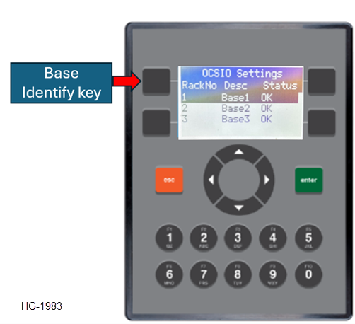
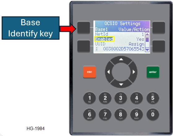
Base Identification from System Menu
This option is to identify the base on field using System Menu of the unit.
-
From the System Menu navigate to View I/O slots > OCS-I/O configuration > OCS-I/O Setting.
-
From the displayed list of configured OCS-I/O bases, select the base with status as “OK”.
-
Click the Identify button onscreen.
-
The identified CNX Base will blink its OK LED @2HZ, for 10 times
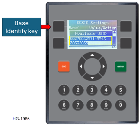
If the program loaded in the device is having different UUID and does not match with the UUID of the currently installed CNX base, then follow these steps to identify the base and assign correct net Id’s as per the requirement.
-
Navigate to System Menu > View I/O slots > OCS-I/O configuration > OCS-I/O Setting.
-
Select the Base from the list of available bases and assign the UUID screen
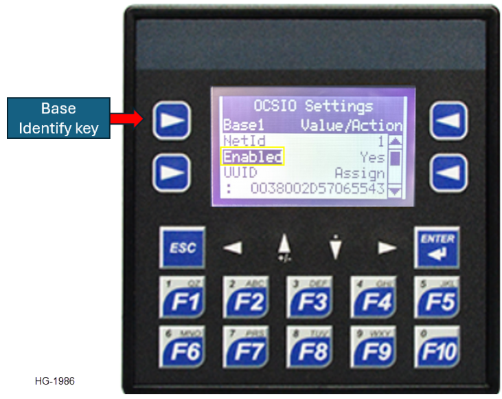
OCSIO Base Identification Feature for X2A/X2R
Base Identification from System Menu
This option is to identify the base on field using system menu of the unit.
-
From the System Menu navigate to View I/O slots -> OCSIO configuration -> OCSIO Setting
-
From the displayed list of configured OCSIO bases, select the base with status as “OK”.
-
Click on “Identify Key” located at Top left side, mentioned in below picture
-
The identified CNX Base will blink its OK LED @ 2Hz, for 10 times.
Navigate inside the base configuration by clicking enter, can see the base configuration and whereby pressing base identify key identified base will blink its OK led @2HZ, for 10times.
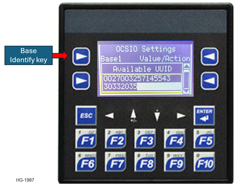
If the program loaded in the device is having different UUID and not matching with the UUID of currently installed CNX base, then follow the below steps to identify the base and assign correct net Id’s as per the requirement.
-
Navigate to System Menu -> View I/O slots -> OCSIO configuration -> OCSIO Setting
-
Select the Base from the list of available bases and go to assign UUID screen as below
-
Select the available UUID and click on Identify key.
-
The identified CNX Base will blink its OK LED @ 2Hz, for 10 times
OCSIO Base Identification Feature for XLE\XLEe Devices
Base Identification from System Menu
This option is to identify the base on field using system menu of the unit.
-
In System Menu -> View I/O slots -> OCSIO configuration -> OCSIO Setting
-
From the displayed list of configured OCSIO bases, select the base with status as “OK”.
-
Click on “Identify Key” located at top left side , mentioned in below picture
-
The identified CNX Base will blink its OK LED @ 2Hz, for 10 times
If the program loaded in the device is having different UUID and not matching with the UUID of currently installed CNX base, then follow the below steps to identify the base and assign correct net Id’s as per the requirement.
-
In System Menu -> View I/O slots -> OCSIO configuration -> OCSIO Setting
-
Select the Base from the list of available bases and go to assign UUID screen as below
-
Select the available UUID and click on Identify button .
-
The identified CNX Base will blink its OK LED @ 2Hz, for 10 times
Return to the Top: OCS-I/O Modules
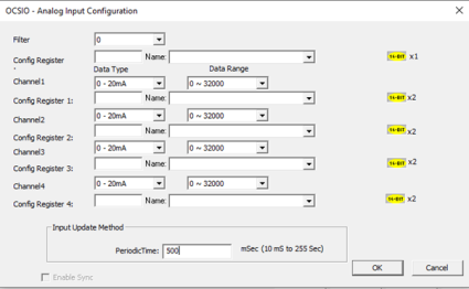
Analog Inputs
Universal In: Check this option to select the universal Analog Inputs type, Data Range and Filter values. If this is unchecked the Analog Input channel will get disabled.
Data Type: Select the Analog Input source data type from the drop down. OCS-I/O CNX base universal Analog Input supports 0-10V,0-20ma,4-20ma,0-60mv, Thermocouples J, K, T, E, N, R, S, B, PT100 and PT1000.
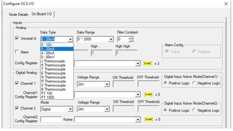
Data Range: Select Data range for the Analog Input. Data range depends on the Input type selected.
| Data Range | |
|---|---|
|
Input Type |
Data Range |
|
0-20mA |
0~4000, -2000~2000,0~1000,0~2000,0~32000 |
|
4-20mA |
0~4000, -2000~2000,0~1000,400~2000,0~32000 |
|
0-10V |
0~4000, -2000~2000,0~1000,0~32000 |
|
0-60mV |
0~4000, -2000~2000,0~1000,0~32000 |
|
Thermocouple J, K, T, E, N, R, S, B |
Degree Celsius and Fahrenheit |
|
PT100 and PT1000 |
Degree Celsius and Fahrenheit |
Filter Constant: Analog Inputs can be filtered Digitally with this Filter constant values. Valid filter values are 0 to 7.
Alarm: OCS-I/O status register has Three bits to indicate Alarm condition of Analog Inputs. User must configure values for Low Low, Low, High and High High to trigger alarm. Once the Analog Input value reaches the Alarm values then the Alarm bit in status Register will get triggered.
| Alarm Bit Registers | |||
|---|---|---|---|
|
ALM Warning |
ALM1 |
ALM0 |
Alarm |
|
1 |
0 |
0 |
LL |
|
0 |
0 |
1 |
L |
|
0 |
0 |
0 |
Normal |
|
0 |
1 |
0 |
H |
|
1 |
1 |
1 |
HH |
Alarm values can be given as a fixed values or through Register. Four consecutive Registers are used for providing alarm values through Registers. See also: System Register Tables
Config Register: Analog Input Type, Data Range, Filter values can be selected through Register. Configure Register in this field and user must move predefined values to the register to select the required Input type, range, and filter.
Note: When Analog Input is configured through Register and Alarm is used as fixed value means, whenever the user changes the data range configuration by changing the dynamic value, the fixed alarm values remain the same and lead to alarm discrepancy. It is recommended to configure Alarm values through Registers if the Universal Analog Input configuration is through Registers.
Return to the Top: OCS-I/O Modules
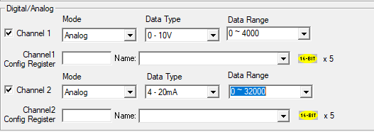
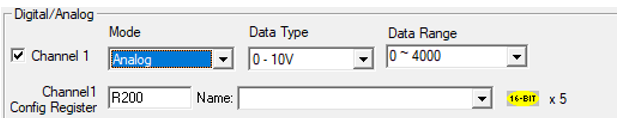
Digital/Analog Inputs
OCS-I/O CNX base supports Two Digital Inputs which can be configured as Analog Inputs also.
-
Channel 1/Channel 2: Check this option to enable Channel 1/Channel 2.
-
Mode: Select the mode of the channel, Digital or Analog
-
Digital Mode: Digital Mode Supports Voltage Range 24V, 12V, 5V and custom ranges.
-
ON and OFF Threshold: In Digital input Custom mode, user can select the Voltage Range to ON and OFF the Input.
-
Digital Input Active Mode: Select the Digital Input source as Positive or Negative Logic for the selected channel.
-
Analog Mode: In Analog Mode each channel supports 0-10V and 4-20mA Input types and Data ranges as in above table (Table 1 Data Range)
-
Config Register: For digital inputs: Voltage Range can be selected by configuring register in this field. Each channel has separate configuration Registers. For Analog Inputs: Mode, Data type and Data Range can be selected by configuring register in this field. Each channel has separate configuration registers.
Return to the Top: OCS-I/O Modules
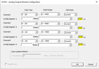
Analog Outputs
OCS-I/O CNX base supports one Analog Output.
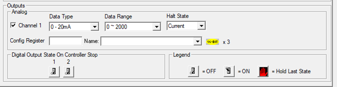
Channel 1: Check this option to select the Analog Outputs type, Data Range and Halt State. If this is unchecked, the Analog Output channel will be disabled.
Data Type: Select the Analog Output data type from the drop down, supported data types are 0-10V,0-20mA and 4-20mA.
Data Range: Select data range for the configured Analog output.
-
Halt State: Select Analog Output value when controller goes to Idle Mode or communication with the host controller get stopped.
-
Current: Output the current value in configured Analog Output Register.
-
Minimum: Output the Minimum value of selected data type.
-
Maximum: Output the maximum value of selected data type.
-
Median: Output the average value of selected data type.
Config Register: Analog Output Type, Data Range and Halt State can be selected through Registers. Configure Register in this field, and user must move predefined values to the register to select the required output type, range, and halt state values.
Digital Output: Select the Digital Output state on controller Stop or communication with host controller get stopped.
DO Halt State:
-
On - Digital Output will On
-
Off - Digital Output will Off
-
Hold - Digital Output will remains in current state
Return to the Top: OCS-I/O Modules
Auto Populate All
Cscape has the feature to automatically detect the connected OCS-I/O CNX base and the attached I/O Modules by using Auto Populate All .
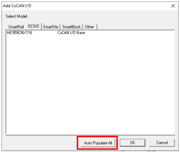
In Add Cscan I/O dialog, click on “Auto Populate All” to detect the connected OCS I/O bases in the Network. Base information will get fetched to Cscape and it will get added in the configuration.
Auto Populate I/O
Cscape also has the feature to automatically detect the connected I/O modules to the Base using Auto Populate I/O. The OCS-I/O CNX base must be manually configured and communication between host controller and base must be established to detect the I/O modules connected to Base.
Click on Auto Populate I/O to detect the I/O modules connected to the Base and once detected the Modules will get added to the configuration in Cscape.
Note: Auto Populate I/O will delete the currently configured I/O modules in Cscape and will get updated with detected I/O modules.
Return to the Top: OCS-I/O Modules
OCS-I/O CNX Base LED Indicators
CNX Status LED
|
CNX Status LED |
||||
|---|---|---|---|---|
|
Status |
Power |
OK (ü) |
MS |
NS |
|
10-30VDC applied |
ON |
ANY |
ANY |
ANY |
|
Self Test fail |
ON |
ANY |
OFF |
ANY |
|
Self Test Pass |
ON |
ANY |
ANY |
ANY |
|
Network Normal |
ON |
ON |
ON |
ON |
|
Duplicate ID |
ON |
ON |
ON |
OFF |
|
Communication Timeout |
ON |
ON |
ON |
Flash (1 HZ) |
|
Configuration Mismatch |
ON |
Flash (1 HZ) |
ON |
Flash (1 HZ) |
|
OCS Stop Mode |
ON |
ON |
ON |
Flash (1 HZ) |
|
OCS Run Mode |
ON |
ANY |
ANY |
ANY |
|
Onboard I/O fault |
ON |
OFF |
ON |
ON |
|
Invalid Dynamic Configuration |
ON |
Flash (1 HZ) |
ON |
ON |
|
Power Up / Waiting to be configured |
ON |
ON |
Flash (1 HZ) |
Flash (1 HZ) |
| Base Identify |
ON |
Flash (2 HZ) |
ANY | ANY |
CNX LED status for Individual I/O Channels
Note: Channel LED will be in OFF state if it is disabled from Cscape configuration.
| Individual I/O Channels | |
|---|---|
|
I1 |
Flexible Input-1 active** |
|
I2 |
Flexible Input-2 active** |
|
Q1 |
Digital Output-1 active |
|
Q2 |
Digital Output-2 active |
|
AI1 |
Analog Input Active * |
|
AQ1 |
Analog output Active |
*
-
LED will be ON during Normal operations.
-
Analog Input channel configured as mA, Volts or mV LED will be OFF till the input signal is 0+0.2%
-
Analog Input channel configured as PT100, PT1000 LED will be OFF if open circuit is detected, LED will be ON during Normal operation
-
Analog Input channel configured as Thermocouple Input LED will be ON if the channel is Enabled.
**
-
Flexible Input channels configured as Digital; LED reflects Digital Input state
-
Flexible Input configured as ma or volts, LED will be OFF till the Input signal is 0+0.2%
Return to the Top: OCS-I/O Modules
OCS-I/O CNX Base Status Registers
OCS-I/O CNX base and stacked IO modules status registers:
| Base Status Registers | ||||||||||||||||
|---|---|---|---|---|---|---|---|---|---|---|---|---|---|---|---|---|
| Register | 16 | 15 | 14 | 13 | 12 | 11 |
10 |
9 | 8 | 7 | 6 | 5 | 4 | 3 | 2 | 1 |
| 1 | IOE | CME | ||||||||||||||
| 2 | IOCS | WDG TRIP | ||||||||||||||
| 3 | Reserved |
NO-CFG |
LIFE ERROR |
ALME |
ALM1 |
ALM0 |
DI2 US |
DI1 US |
OFFLINE |
PUP | ||||||
| 4 | IO Base Net ID | |||||||||||||||
| 5 |
IO Base Type |
|||||||||||||||
| 6 |
IO Base Scan Rate |
|||||||||||||||
| 7 |
IO Base Watchdog Trip Count |
|||||||||||||||
| 8-15 | FPGA(HSC840) & FW Version (Base & All IO Modules) | |||||||||||||||
CME- Each bit (bit1 – bit8) represents configuration mismatch error of each IO modules (Module 1 to Module 8)
-
IOE – Each bit (bit9 – bit 16) represents IO modules error (Module 1 to Module 8)
-
WDG TRIP – IO base watchdog trip count
-
IOCS- Each bit (bit9 – bit 16) represents IO modules calibration status (Module 1 to Module 8)
-
PUP – Power up error (sticky bit)
-
OFFLINE – OCS-I/O is offline
-
DI1 US - High when Digital input 1 is in undefined state
-
DI2 US – High when Digital input 2 is in undefined state, e.g.,: If 24V input range selected then I1 US bit set if voltage between 8V to 16V
-
ALE- Alarm Error
-
ALM0 – Alarm Bit
-
ALM1 – Alarm bit
-
LIFE ERROR – sticky bit set when OCS-I/O went to offline and back to online
-
NO CFG – OCS-I/O configuration status
Return to the Top: OCS-I/O Modules
| Register | Description |
|---|---|
| %Rx | CME- Each bit (bit8 – bit1) represents communication error of each IO modules (Module 8 to Module 1) |
| IOE – Each bit (bit16 – bit 9) represents IO modules error (Module 8 to Module 1) | |
| %Rx+1 | WDG TRIP – Base watchdog trip |
| IOCS- Each bit (bit9 – bit 16) represents IO modules calibration status (Module 8 to Module 1) | |
| %Rx+2 | PUP – Power up error (sticky bit) |
| OFFLINE – OCS-I/O is offline | |
| DI1 US - High when Digital input 1 is in undefined state | |
|
DI2 US – High when Digital input 2 is in undefined state E.g., If 24V input range selected then I1 US bit set if voltage between 8V to 16V |
|
| ALM0 – Alarm bit | |
| ALM1 – Alarm Bit | |
| ALE- Alarm Error | |
| LIFE ERROR – sticky bit set when OCS-I/O went to offline and back to online | |
| NO CFG – OCS-I/O configuration status | |
| %R8+15 |
Firmware version of the connected OCS-I/O modules. For the HSC840 Module, the FPGA version and FW version are shown in the same Status Register.
|
Digital Input Module
DIM620: Supports 8 Digital Inputs with AC voltage active Range 80-260VAC.
Update Method: An I/O Module with digital inputs can be configured to update its digital input data either on change of state or periodically. The update period is programmable from 10 mS to 255 Seconds.
Return to the Top: OCS-I/O Modules
Mixed Digital Modules
DIQ512: Supports 4-point Digital Inputs and 4 Relay Output
DIQ616: Supports 8-point Digital Inputs and 8-point 24V DC Output
-
Filter: Select the filter settings, for digital input modules. The changes in input state less than this setting are not reflected in the configured register.
-
Update Method: An I/O Module with digital inputs can be configured to update its digital input data either on change of state or periodically. The update period is programmable from 10 mS to 255 Seconds
-
Digital Input Active Mode: Select the mode for Digital Input signal as either positive or Negative Logic.
-
Digital Output on Controller Stop: Digital outputs normally turn off if communication is lost with the Host Controller or if the Host Controller goes into IDLE mode. However, digital outputs can optionally be configured to hold last state or Turn ON instead.
Return to the Top: OCS-I/O Modules
Digital Output Module
DQM502: Supports 4 Relay output
Digital Output on Controller Stop: Digital outputs normally turn off if communication is lost with the Host Controller or if the Host Controller goes into IDLE mode. However, digital outputs can optionally be configured to hold last state or Turn ON instead.
Return to the Top: OCS-I/O Modules
Analog Input Module
ADU100: Supports 4 channel Analog Inputs
-
Filter Constant: Analog Inputs can be filtered Digitally with this Filter constant values. Valid filter values are 0 to 7.
-
Data Type: Select the input Data Type as voltage / current/Thermocouple/RTD from the dropdown list. Each analog input channel can be Disabled by selecting option” Disable” in the drop-down menu.
-
Data Range: Select the data range for the input. Analog input is scaled based on the Data type and Data range selected; and reflected in the configured register.
Note: Refer the Data Range table in Analog Inputs for analog input supported data type and data range.
-
Input Update Method: An I/O Module with analog inputs always updates its analog input data periodically. The update period is programmable from 10 mS to 255 Seconds.
-
Analog Input type, Data Range, Filter values can be selected through Register. Configure register in this field and user must move predefined values to the register to select the required input type, range and filter.
Return to the Top: OCS-I/O Modules
Analog Output Module
DAC107: Supports 4 channel Analog outputs
| Data Range | |
| Output Type | Data Range |
| -10 - +10V | 0~4000, -2000~2000,0~1000,0~32000 |
| 0-10V | 0~4000, -2000~2000,0~1000,0~32000 |
| 0-20mA | 0~4000, -2000~2000,0~1000,0~2000,0~32000 |
| 4-20mA | 0~4000, -2000~2000,0~1000,400~2000,0~32000 |
-
Data Type: Select the Analog Output range from the dropdown list
-
Data Range: Select the data range for the analog output from the dropdown list. The analog output will be scaled according to the data in the configured register, selected data type and data range. Each analog Output channel can be Disabled by selecting option” Disable” in the dropdown
-
Halt State: Each analog output can be configured to either hold its current value or go to minimum, Average or maximum value, if communication is lost with the Host Controller or if the Host Controller goes into IDLE mode.
-
Analog Output type, Data Range, halt state values can be selected through Register. Configure register in this field and user must move predefined values to the register to select the required output type, range and halt state.
Return to the Top: OCS-I/O Modules
Dynamic I/O Configuration: Definition for Onboard I/O
Config Register: If a Config Register is configured, it takes immediate precedence over other configuration for the I/O, thus requiring valid values in the registers. These values can be changed during runtime, so care needs to be taken to not mistakenly overwrite these values and program logic.
Return to the Top: OCS-I/O Modules
Analog Input: Universal In
Analog Input uses three consecutive 16-Bit registers for configuration and each register has the following description:
As an example, if %R100 is configured for Analog Inputs:
-
Universal AI Data type- %R100
Data Type Value 0-10V 0 0-20mA 1 4-20mA 2 0-60mV 3 J Thermocouple 4 K Thermocouple 5 T Thermocouple 6 E Thermocouple 7 N Thermocouple 8 R Thermocouple 9 S Thermocouple 10 B Thermocouple 11 PT100 12 PT1000 13 -
Universal AI Data Range-- %R101
0-10V Range
0-20mA Range
4-20mARange 0-60mV Range
RTD Thermocouples Value 0~4000 0~4000 0~4000 0~4000 Reserved
Reserved
0
-2000~2000 -2000~2000 -2000~2000 -2000~2000 Reserved
Reserved
1
0~1000 0~1000 0~1000 0~1000 Reserved
Reserved
2
Reserved 0~2000 Reserved Reserved Reserved
Reserved
3
Reserved Reserved 400~2000 Reserved Reserved
Reserved
4
0~32000 0~32000 0~32000 0~32000 Reserved
Reserved
5
Reserved Reserved Reserved Reserved Reserved
Reserved
6
Reserved Reserved Reserved Reserved °C
°C
7
Reserved Reserved Reserved Reserved °F
°F
8
-
Universal AI Filter Constants (0 to 7)- % R102
Return to the Top: OCS-I/O Modules
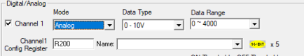
Analog Input: Universal In
Flexible Input uses five consecutive 16-Bit registers for configuration and each register has the following description:
As an example, if %R200 is configured for Digital Inputs Channel 1. Consider if Channel 1 is selected Analog:
-
Channel 1 Mode- %R200
Mode Value Digital 0 Analog 1 -
Channel 1 Data Type- %R201
Data Type Value 0-10V 0 4-20mA 2 -
Channel 1 Data range- %R202
0-10V Range 4-20mA Range
Value 0~4000 0~4000 0
-2000~2000 -2000~2000 1
0~1000 0~1000 2
Reserved Reserved 3
Reserved 400~2000 4
0~32000 0~32000 5
Return to the Top: OCS-I/O Modules
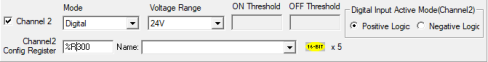
Digital/Analog Channel 2
As an example, if %R300 is configured for Digital Inputs channel 2. Consider if Channel 2 is selected as Digital:
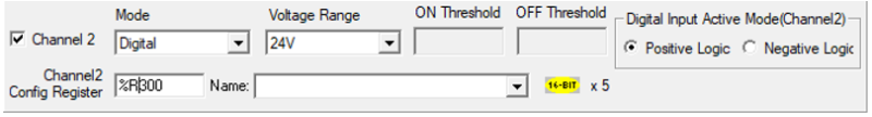
-
Channel 2 Mode as Digital: %R300
Mode Value Digital 0 Analog 1 -
Channel 2 Voltage Range: %R301
Voltage Range
Value
24V
0
12V
1
5V
2
Custom
3
-
Channel 2 ON Threshold (5 to 20): %R302
-
Channel 2 OFF Threshold (5 to 20): %R303
Note: ON Threshold should be greater than OFF Threshold in Positive logic
Note: OFF Threshold should be greater than ON Threshold in Negative logic
-
Active Mode: %R304
Mode Value Positive Logic 0 Negative Logic 1
Return to the Top: OCS-I/O Modules
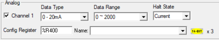
Analog Output Channel;
Analog Output uses three consecutive 16-Bit registers for configuration and each register has the following description. As an example, if %R400 is configured for Analog Output channel:
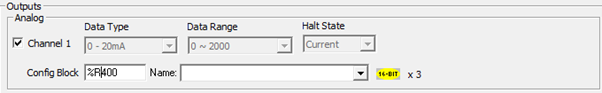
-
Analog Output data type: %R400
Data Type Value 0-10V 0 0-20mA 1 4-20mA 2 -
Analog Output Data Range: %R401
0-10V Range 0-20mA Range
4-20mA Range
Value 0~4000 0~4000 0~4000 0
-2000~2000 -2000~2000 -2000~2000 1
0~1000 0~1000 0~1000 2
Reserved 0~2000 Reserved 3
Reserved Reserved 400~2000 4
0~32000 0~32000 0~32000 5
-
Analog Output Halt State: %R402
Halt State
Value
Current
0
Minimum
1
Maximum
2
Average
3
-
Analog Output Module
Data Range
Output Type Data Range -10 - +10V
0~4000, -2000~2000,0~1000,0~32000
0-10V
0~4000, -2000~2000,0~1000,0~32000
0-20mA
0~4000, -2000~2000,0~1000,0~2000,0~32000
4-20mA
0~4000, -2000~2000,0~1000,400~2000,0~32000
Return to the Top: OCS-I/O Modules
CNX116 Dynamic I/O Configuration
a. Analog Input: Universal In
Analog Input uses three consecutive 16-Bit registers for configuration and each register has the following description. As an example, if %R100 is configured for Analog Inputs
Universal AI Data Type- %R100
| Data Type | Value |
| 0-10V | 0 |
| 0-20mA | 1 |
| 4-20mA | 2 |
| 0-60mV | 3 |
| J Thermocouple | 4 |
| K Thermocouple | 5 |
| T Thermocouple | 6 |
| E Thermocouple | 7 |
| N Thermocouple | 8 |
| R Thermocouple | 9 |
| S Thermocouple | 10 |
| B Thermocouple | 11 |
| PT100 | 12 |
| PT1000 | 13 |
Universal AI Data Range - %R101
| 0-10V Range | 0-20 mA Range |
4-20mA Range |
0-60mV Range |
RTD | Thermocouple | Value |
| 0~4000 | 0~4000 | 0~4000 | 0~4000 | Reserved | Reserved | 0 |
| -2000~2000 | -2000~2000 | -2000~2000 | -2000~2000 | Reserved | Reserved | 1 |
| 0~1000 | 0~1000 | 0~1000 | 0~1000 | Reserved | Reserved | 2 |
| Reserved | 0~2000 | Reserved | Reserved | Reserved | Reserved | 3 |
| Reserved | Reserved | 400~2000 | Reserved | Reserved | Reserved | 4 |
| 0~32000 | 0~32000 | 0~32000 | 0~32000 | Reserved | Reserved | 5 |
| Reserved | Reserved | Reserved | Reserved | Reserved | Reserved | 6 |
| Reserved | Reserved | Reserved | Reserved | ºC | ºC | 7 |
| Reserved | Reserved | Reserved | Reserved | ºF | ºF | 8 |
Universal AI Data Range - %R101
Filter Constant Values 0 to 7.
b. Digital/Analog Channel 1
Flexible Input uses five consecutive 16-Bit registers for configuration and each register has the following description: As an example, if %R200 is configured for Digital Inputs channel 1
Consider if Channel 1 is selected Analog
Channel 1 Mode - %R200
| Mode | Value |
| Digital | 0 |
| Analog | 1 |
Channel 1 Data Type - %R201
| Data Type | Value |
| 0-10V | 0 |
| 4-20mA | 2 |
Channel 1 Data Type - %R202
| 0-10V Range | 4-20mA Range | Value |
| 0~4000 | 0~4000 | 0 |
| -2000~2000 | -2000~2000 | 1 |
| 0~1000 | 0~1000 | 2 |
| Reserved | Reserved | 3 |
| Reserved | 400~2000 | 4 |
| 0~32000 | 0~32000 | 5 |
c. Digital/Analog Channel 2
As an example, if %R300 is configured for Digital Inputs channel 2. Consider if Channel 2 is selected Digital.
Channel 2 Mode as Digital - %R300
| Mode | Value |
| Digital | 0 |
| Analog | 1 |
Channel 2 Voltage Range - %R301
| Voltage Range | Value |
| 24V | 0 |
| 12V | 1 |
| 5V | 2 |
| Custom | 3 |
Channel 2 ON Threshold (5 to 20) - %R302
Channel 2 OFF Threshold (5 to 20) - %R303
Note:
1. ON Threshold should be greater than OFF Threshold in Positive logic.
2. OFF Threshold should be greater than ON Threshold in Negative logic.
Active Mode - %R304
| Mode | Value |
| Positive Logic | 0 |
| Negative Logic | 1 |
d. Analog Output Channel
Analog Output uses three consecutive 16-Bit registers for configuration and each register has the following description:
As an example, if %R400 is configured for Analog Output channel
Analog Output Data Type - %R400
| Data Type | Value |
| 0-10V | 0 |
| 0-20mA | 1 |
| 4-20mA | 2 |
Analog Output Data Range - %R401
| 0-10V Range | 0-20mA Range | 4-20mA Range | Value |
| 0~4000 | 0~4000 | 0~4000 | 0 |
| -2000~2000 | -2000~2000 | -2000~2000 | 1 |
| 0~1000 | 0~1000 | 0~1000 | 2 |
| Reserved | 0~2000 | Reserved | 3 |
| Reserved | Reserved | 400~2000 | 4 |
| 0~32000 | 0~32000 | 0~32000 | 5 |
Analog Output Halt State - %R402
| Halt State | Value |
| Current | 0 |
| Minimum | 1 |
| Maximum | 2 |
| Average | 3 |
ADU100 Dynamic I/O Configuration
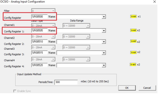
a. AI Filter Constants - %R500
ADU100 Module AI channel Filter Constant Values 0 to 7 which is common for all 4 channels.
b. AI Data Type - %R505
ADU100 Analog Input uses two consecutive 16-Bit registers for configuration and each register has the following description. As an example, if %R500 is configured for Analog Inputs
| Data Type | Value |
| 0-10V | 0 |
| 0-20mA | 1 |
| 4-20mA | 2 |
| 0-60mV | 3 |
| J Thermocouple | 4 |
| K Thermocouple | 5 |
| T Thermocouple | 6 |
| E Thermocouple | 7 |
| N Thermocouple | 8 |
| R Thermocouple | 9 |
| S Thermocouple | 10 |
| B Thermocouple | 11 |
| PT100 | 12 |
| PT1000 | 13 |
| Disable | 14 |
c. AI Data Range - %R506
| 0-10V Range | 0-20 mA Range |
4-20mA Range |
0-60mV Range |
RTD | Thermocouple | Value |
| 0~4000 | 0~4000 | 0~4000 | 0~4000 | Reserved | Reserved | 0 |
| -2000~2000 | -2000~2000 | -2000~2000 | -2000~2000 | Reserved | Reserved | 1 |
| 0~1000 | 0~1000 | 0~1000 | 0~1000 | Reserved | Reserved | 2 |
| Reserved | 0~2000 | Reserved | Reserved | Reserved | Reserved | 3 |
| Reserved | Reserved | 400~2000 | Reserved | Reserved | Reserved | 4 |
| 0~32000 | 0~32000 | 0~32000 | 0~32000 | Reserved | Reserved | 5 |
| Reserved | Reserved | Reserved | Reserved | Reserved | Reserved | 6 |
| Reserved | Reserved | Reserved | Reserved | ºC | ºC | 7 |
| Reserved | Reserved | Reserved | Reserved | ºF | ºF | 8 |
ADC270: Supports 8 channel (0-10V/ 0-20mA/ 4-20mA) Analog Inputs
-
Filter Constant: Analog Inputs can be filtered Digitally with this Filter constant values. Valid filter values are 0 to 7.
-
Data Type: Select the input Data Type as 0-10V/ 0-20 mA/ 4-20mA. Each analog input channel can be Disabled by selecting option” Disable” in the dropdown menu.
-
Data Range: Select the data range from the dropdown for the input. Analog input is scaled based on the Data type and Data range selected; and reflected in the configured register.
| Data Range | |
|---|---|
|
Input Type |
Data Range |
|
0-20mA |
0~4000, -2000~2000,0~1000,0~2000,0~32000 |
|
4-20mA |
0~4000, -2000~2000, 0~1000, 400~2000, 0~32000 |
|
0-10V |
0~4000, -2000~2000,0~1000,0~32000 |
-
Input Update Method: An I/O Module with analog inputs always updates its analog input data periodically. The update period is programmable from 10 mS to 255 Seconds.
-
Analog Input type, Data Range, Filter values can be selected through Register. Configure register in this field and user must move predefined values to the register to select the required input type, range and filter.
Return to the Top: OCS-I/O Modules
DAC107 Dynamic I/O Configuration
DAC module Analog Output uses three consecutive 16-Bit registers for configuration and each register has the following description: As an example, if %R600 is configured for Analog Output channel.
-
Analog Output data type: %R600
Data Type Value -10V, +10V 0 0-10V 1 0-20mA 2 4-20mA 3 Disable 4 -
Analog Output Data Range: %R601
-10V, +10V Range 0-10V Range 0-20mA Range
4-20mA Range
Value 0~4000 0~4000 0~4000 0~4000 0
-2000~2000 -2000~2000 -2000~2000 -2000~2000 1
0~1000 0~1000 0~1000 0~1000 2
Reserved Reserved 0~2000 Reserved 3
Reserved Reserved Reserved 400~2000 4
0~32000 0~32000 0~32000 0~32000 5
-
Analog Output Halt State: %R602
Halt State
Value
Current
0
Minimum
1
Maximum
2
Average
3
ADC270 Dynamic I/O Configuration
-
AI Filter Constants - %R700: ADC270 Module AI channel Filter Constant Values 0 to 7 which is common for all 4 channels.
-
AI Data Type - %R705: ADC270 Analog Input uses two consecutive 16-Bit registers for configuration and each register has the following description. As an example, if %R705 is configured for Analog Inputs.
| Data Type | Value |
| 0-10V | 0 |
| 0-20mA | 1 |
| 4-20mA | 2 |
| Disable | 14 |
c. AI Data Range - %R706
| 0-10V Range | 0-20 mA Range | Value |
| 0~4000 | 0~4000 | 0 |
| -2000~2000 | -2000~2000 | 1 |
| 0~1000 | 0~1000 | 2 |
| Reserved | 0~2000 | 3 |
| Reserved | Reserved | 4 |
| 0~32000 | 0~32000 | 5 |
| Reserved | Reserved | 6 |
| Reserved | Reserved | 7 |
| Reserved | Reserved | 8 |
Return to the Top: OCS-I/O Modules
HSC840 Dynamic I/O Configuration
See High Speed I/O General Overview and Defaults for an overview of terms and default HSC information. The information in this section may be different as it is specific to the HSC840.
The HSC840 contains a Field-Programmable Gate Array (FPGA), which is an integrated configurable circuit that allows the HSC840 to be programmed to have up to eight high-speed counters. The high-speed counters can be configured as normal inputs or high-speed inputs, with four high-speed outputs that can be configurable as normal outputs or PWM, or Stepper (or PTO outputs). In high-speed output PWM functions include traditional PWM (with variable frequency and duty cycle) and a stepper or PTO (Pulse Train Output) functionalities with variable acceleration and deceleration rates.
High Speed Counter (HSC) Functions
The HSC840 supports eight high-speed, configurable counters. There are eight dedicated inputs that can be configured for a number of different options. Each of the eight counters can run in one of five modes. Those modes are Totalizer, Frequency Counter, Pulse Width Measurement, Period Measurement, and Quadrature measurement. For some modes, more than one HSC input may be required. The measurement values are provided to the ladder in a %AI register.
Frequency Mode
In frequency mode, the frequency of the input signal is written to the accumulator in terms of Hertz (cycles/second). When using frequency mode, four update selections are provided which specify the width of the sample window.
NOTE: Selecting a shorter sample window provides a quicker measurement (faster response) but lowers the frequency accuracy (resolution) and increases the minimum frequency measurement limit. In this mode the Disable and Latch special functions are allowed.
Totalize Mode
In totalize mode, the accumulator is simply incremented or decremented each time the input transitions in a specific direction. The totaliser supports the following modes:
|
Internal |
This mode ties the input to the counter to an internal 10MHz or 1MHz clock. The special functions can be used to accurately time events. |
|
This mode increments the accumulator NOTE: Two inputs can be assigned. Either input can cause the counter to increment. The second input can also be disabled. |
|
|
This mode decrements the accumulator when the input is enabled. NOTE: Two inputs can be assigned. Either input can cause the counter to decrement. The second input can also be disabled. |
|
|
Up/Down (Input 1 Up/Input 2 Down) |
In this mode, input 1 (assigned to any of the eight inputs) increments the counter, while input 2 (also assigned to any of the eight inputs) decrements the counter. |
|
Clk/Dir (Input 1 Clk, Input 2 Dir) |
This mode uses input 1 as a clock signal to increment or decrement the counter and then uses input 2 to decide the direction. Input 2 disabled increments the counter, while input 2 enabled decrements the counter. |
NOTE: The counter triggers on the rising edge of the signal.
Resetting the Current Count
Three options are available to reset the current count. They are:
-
When configuring the Totalize function, a value may be specified under the Counts per Rev column. When the totalizer accumulator reaches this value - 1, the accumulator will reset to zero on the next count. Specifying zero for this value allows the totalizer to count through the full 32-bit range before resetting.
-
Setting registers %Q17-20 reset HSC1-4 (respectively) with no additional configuration. When these registers are asserted, the associated totalizer accumulator is reset and held at zero (level sensitive).
-
(HSC1 and HSC2 only) - HSC3 (%I11) and HSC4 (%I12) may be configured as hardware digital reset signals for HSC1 and HSC2 (respectively). To enable these inputs as reset signals, specify the type as Totalize Reset (NOTE: The corresponding Totalize counter must be previously configured before this option is available). The direct digital reset controls are edge sensitive with the edge polarity configurable.
Maximum Direct Digital Reset Latency is 100μs.
The totalize function also supports an option which compares the current accumulator value with a supplied Preset Value (PV), which is provided through a %AQ, and drives a physical digital output based on the that comparison.
NOTE: This option (available for HSC1 and HSC2 only) drives Q1 or Q2 output point (respectively) once the asso-ciated totalizer accumulator reaches (or exceeds) the PV value. To enable this function, the corresponding PWM function output (Q1 or Q2) must be configured for HSCx Output.
NOTE: Q1 and Q2 are PWM function outputs that may be configured independently as one of the following: stand- ard digital output, PWM, HSCx or stepper output.
Preset values may be modified during run-time. A preset value of zero disables (resets) the totalizer compares function output causing the output to remain low.
Pulse Width Measurement or PWM
In Pulse Width Measurement mode, the high-speed input can measure the width of a pulse stream in one of two modes and provides a continuous indication of the last sampled value. In this mode the Disable![]() When the disable function is active it will “disable” the high-speed inputs and no longer count pulses until it is re-enabled. and Latch
When the disable function is active it will “disable” the high-speed inputs and no longer count pulses until it is re-enabled. and Latch![]() When the Latch function is active it takes the current value of the Accumulator and moves it into the “Latch Value” register special functions are allowed.
When the Latch function is active it takes the current value of the Accumulator and moves it into the “Latch Value” register special functions are allowed.
-
Width High 1μs Counts – In this sub-mode the accumulator
 A register/variable used to gather or accumulate a total of time, counts, items, or events. value will contain the number of 1μs counts the pulse is high.
-
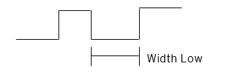
Width Low 1μs Counts - In this sub-mode the accumulator value will contain the number of 1μs counts the pulse is low.
Period Measurement
In period measurement mode, the high-speed input can measure the period of a pulse stream in one of two modes and provides a continuous indication of the last sampled value. In this mode, the Disable and Latch special functions are allowed. Refer to the "High Speed I/O Glossary " on page 98 for a description of these functions.
-
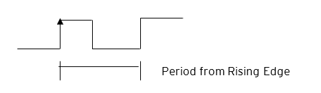
Period Rising Edges 1μs Counts – In this sub-mode the period of the input signal is reported in one (1) μs units. The period measurement will start on the rising edge of the input.
-
Period Falling Edges 1μs Counts – In this sub-mode the period of the input signal is reported in one (1) μs units. The period measurement will start on the falling edge of the input.

Quadrature
Quadrature![]() Separation in phase by two pulses of 90°. Used on signal channel of feedback devices to detect the direction of motion. mode uses two HSC inputs, any of the four HSC inputs can be assigned for this purpose.
Separation in phase by two pulses of 90°. Used on signal channel of feedback devices to detect the direction of motion. mode uses two HSC inputs, any of the four HSC inputs can be assigned for this purpose.
Quadrature mode works much like the Totalize function except the accumulator![]() A register/variable used to gather or accumulate a total of time, counts, items, or events. will automatically increment or decrement based on the rotation phase of the two inputs. See the following example for more details. Quadrature inputs are typically used for reporting the value of an encoder.
A register/variable used to gather or accumulate a total of time, counts, items, or events. will automatically increment or decrement based on the rotation phase of the two inputs. See the following example for more details. Quadrature inputs are typically used for reporting the value of an encoder.
Two modes are available for quadrature that select whether the accumulator counts up or down when the phase of input 1 leads input 2. Check the encoder’s documentation to determine the output form it uses or try both modes to determine if the encoder counts up when expected.
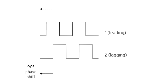
Using the above waveforms and a HSC input configuration of “Quadrature” - “1 leads 2, count up,” the accumulator will count up when 1 is rising and 2 is low, 1 is high and 2 is rising, 1 is falling and 2 is high, and when 1 is low and 2 is falling. This results in 4 counts per revolution. In order to determine the number of cycles, the accumulator would have to be divided by 4.
The Marker reset operation is configured in the special operations and can be assigned to any of the 4 high speed inputs or can be assigned to be controlled by a “Q” bit in ladder.
Note: The quadrature mode enables the Disable![]() When the disable function is active it will “disable” the high-speed inputs and no longer count pulses until it is re-enabled., Latch
When the disable function is active it will “disable” the high-speed inputs and no longer count pulses until it is re-enabled., Latch![]() When the Latch function is active it takes the current value of the Accumulator and moves it into the “Latch Value” register, Preload
When the Latch function is active it takes the current value of the Accumulator and moves it into the “Latch Value” register, Preload![]() When the pre-load function is active it will take the value from the “Preload” register and put it into the “Accumulator” for the corresponding Counter., Clear
When the pre-load function is active it will take the value from the “Preload” register and put it into the “Accumulator” for the corresponding Counter., Clear![]() When the clear function is active it will move a value of 0 into the “Accumulator” for the corresponding counter., and Marker
When the clear function is active it will move a value of 0 into the “Accumulator” for the corresponding counter., and Marker![]() When the marker function is enabled, it acts as a dynamic enable/disable for the Disable, Latch, Preload and Clear functions. So, if the marker is enabled and “Assigned %Q” is selected then both the “Disable” and the “Disable Marker” bits need to be set high in order to disable the high-speed input. If the Marker is set for one of the inputs then the input will need to be “High” in order to use any of the Disable, clear, preload, or Latch functions. special functions.
When the marker function is enabled, it acts as a dynamic enable/disable for the Disable, Latch, Preload and Clear functions. So, if the marker is enabled and “Assigned %Q” is selected then both the “Disable” and the “Disable Marker” bits need to be set high in order to disable the high-speed input. If the Marker is set for one of the inputs then the input will need to be “High” in order to use any of the Disable, clear, preload, or Latch functions. special functions.
Register Match
Totalizer![]() A counter that sums the total number of cycles applied to its input. and Quadrature
A counter that sums the total number of cycles applied to its input. and Quadrature![]() Separation in phase by two pulses of 90°. Used on signal channel of feedback devices to detect the direction of motion. counter modes support a Register Match function. When the accumulator
Separation in phase by two pulses of 90°. Used on signal channel of feedback devices to detect the direction of motion. counter modes support a Register Match function. When the accumulator![]() A register/variable used to gather or accumulate a total of time, counts, items, or events. value matches either the Match 1 or Match 2 value configured in the corresponding %AQ
A register/variable used to gather or accumulate a total of time, counts, items, or events. value matches either the Match 1 or Match 2 value configured in the corresponding %AQ![]() 16-bit output registers used to send analog information such a voltages, levels, or speed settings to an attached device. registers, a high-speed output can Turn On, Turn Off, or Toggle. An internal %I
16-bit output registers used to send analog information such a voltages, levels, or speed settings to an attached device. registers, a high-speed output can Turn On, Turn Off, or Toggle. An internal %I![]() Single-bit input registers. Typically, an external switch is connected to the registers. register mirrors the output state whether the high-speed output is configured or not. The output can be reset in program logic using the corresponding %Q
Single-bit input registers. Typically, an external switch is connected to the registers. register mirrors the output state whether the high-speed output is configured or not. The output can be reset in program logic using the corresponding %Q![]() Single-bit output registers. Typically, these bits are connected to an actuator, indicator light or other physical outputs. registers.
Single-bit output registers. Typically, these bits are connected to an actuator, indicator light or other physical outputs. registers.
-
2-Counter Mode has Register Match support for both counters.
-
4-Counter Mode has Register Match support only for counters 1 and 2.
-
The High-Speed Outputs are %Q1 for Counter 1 and %Q2 for Counter 2. They operate as high-speed outputs, independent of the controller scan rate, when configured as ‘HSC Output’ in the Digital Out/PWM
Pulse Width Modulation (PWM) - A technique for generating a DC voltage level from a higher constant DC voltage. The constant input voltage is chopped to produce pulses at a constant period and constant amplitude. Modulating the pulse width (duration) controls the average voltage of the output. configuration in Cscape. -
The High-Speed Output state reflects in the status register “High Speed Out”, e.g. %I1603 for Counter 1 (the update speed of the status bit is scan rate dependent)
-
The High-Speed Output can be reset through ladder with the assigned output, e.g. %Q1606 for Counter 1
-
Both Match 1 and Match 2 values will trigger the match function.
-
If the output is already triggered by any Match register while using ‘Turn On’ or ‘Turn Off’ modes, subsequent matches will not affect the output.
-
If using ‘Toggle’ mode, every match of either Match value will toggle the output to the opposite state.
HSC Functions
The high-speed input on an OCS contains many optional tasks, all of which can be disabled, or set to an internal pre-assigned register (Assigned %Q) or to one of the external High-speed inputs (External Input #1, 2, 3 or 4).
Also, they can be set as an “overflow interrupt” or “underflow interrupt” meaning that they will occur when either the Overflow, or Underflow input has been activated.
-
Disable
When the disable function is active it will “disable” the high-speed inputs and no longer count pulses until it is re-enabled.: When the disable function is active it will “disable” the high-speed inputs and no longer count pulses until it is re-enabled -
Latch
When the Latch function is active it takes the current value of the Accumulator and moves it into the “Latch Value” register: When the Latch function is active it takes the current value of the Accumulator and moves it into the “Latch Value” register -
Preload
When the pre-load function is active it will take the value from the “Preload” register and put it into the “Accumulator” for the corresponding Counter.: When the preload function is active it will take the value from the “Preload” register and put it into the “Accumulator A register/variable used to gather or accumulate a total of time, counts, items, or events.” for the corresponding Counter. -
Clear
1. To zero out one or more variables/registers.
2. To delete the contents in memory, such as the program in an OCS.: When the clear function is active it will move a value of 0 into the “Accumulator” for the corresponding counter -
Marker
When the marker function is enabled, it acts as a dynamic enable/disable for the Disable, Latch, Preload and Clear functions. So, if the marker is enabled and “Assigned %Q” is selected then both the “Disable” and the “Disable Marker” bits need to be set high in order to disable the high-speed input. If the Marker is set for one of the inputs then the input will need to be “High” in order to use any of the Disable, clear, preload, or Latch functions.: When the marker function is enabled, it acts as a dynamic enable/disable for the Disable, Latch, Preload and Clear functions. So, if the marker is enabled and “Assigned %Q” is selected then both the “Disable” and the “Disable Marker” bits need to be set high in order to disable the high-speed input. If the Marker is set for one of the inputs then the input will need to be “High” in order to use any of the Disable, Clear, Preload, or Latch functions.
HSC Status Bits
There are three status bits ( %I![]() Single-bit input registers. Typically, an external switch is connected to the registers. registers for each high-speed counter):
Single-bit input registers. Typically, an external switch is connected to the registers. registers for each high-speed counter):
-
Overflow Flag: This status bit turns high when the Accumulator “overflows”, it moves from 4,294,967,295 (-1 if Signed) to 0, this bit can be reset with the Output Reset Bit.
-
Underflow Flag: This status bit turns high when the Accumulator “underflows”, it moves from 0 to 4,294,967,295 (-1 if Signed), this bit can also be reset with the “Output Reset Bit”. NOTE: For the Overflow and Underflow flag registers, if using some sort of counter that counts both up and down, going over the threshold to go negative, triggers the underflow, and then going back over the threshold back into positive numbers will trigger the positive register to go active.
-
High-Speed Out: This register will follow the high-speed output assigned to the counter, it is important to note that this register is still populated within the scan time
Time required for the controller to read its inputs, solve the Ladder Logic program, and write its outputs. Scan times are usually expressed in milliseconds.
NOTE: Scan times can vary, depending on number and complexity of Ladder Logic rungs that are active during the "solve" portion of the scan. so the value in this register may not be up to date depending on the timing of the output; it should be up to date within one scan.
HSC Functions Register Assignments
The register assignments for the high-speed I/O can be moved using a setting in Cscape. The values shown are the DEFAULT values and may not match the same starting point as the values shown below.
HSC Functions Register Map
-
The default register address is shown in column 1,
-
The address in column 2 is the default + an optional offset ‘x’.
-
X is any value that keeps the bit addresses on a word boundary and that keeps the highest register within the controller register range
|
Default |
Register |
Description |
|---|---|---|
| AI1 | %AIx+0-1 | HSC1 Accumulator |
| %AI3 | %Aix+2-3 | HSC1 Latched Accumulator |
| %AI5 | %AIx+4-5 | HSC2 Accumulator |
| %AI7 | %AIx+6-7 | HSC2 Latched Accumulator |
| %AI9 | %AIx+8-9 | HSC3 Accumulator |
| %AI11 | %AIx+10-11 | HSC3 Latched Accumulator |
| %AI13 | %AIx+12-13 | HSC4 Accumulator |
| %AI15 | %AIx+14-15 | HSC4 Latched Accumulator |
| %AI17 | %AIx+16-17 | HSC5 Accumulator |
| %AI19 | %AIx+18-19 | HSC5 Latched Accumulator |
| %AI21 | %AIx+20-21 | HSC6 Accumulator |
| %AI23 | %AIx+22-23 | HSC6 Latched Accumulator |
| %AI25 | %AIx+24-25 | HSC7 Accumulator |
| %AI27 | %AIx+26-27 | HSC7 Latched Accumulator |
| %AI29 | %AIx+28-29 | HSC8 Accumulator |
| %AI31 | %AIx+30-31 | HSC8 Latched Accumulator |
|
Default Register |
Register |
Description |
|---|---|---|
| AQ1 | %AQx+0-1 | HSC1 Preload Value |
| %AQ3 | %AQx+2-3 | HSC1 Match 1 Value |
| %AQ5 | %AQx+4-5 | HSC1 Match 2 Value / Pulse Width HSC1 (in micro sec) |
| %AQ7 | %AQx+6-7 | HSC2 Preload Value |
| %AQ9 | %AQx+8-9 | HSC2 Match 1 Value |
| %AQ11 | %AQx+10-11 | HSC2 Match 2 Value / Pulse Width HSC2 (in micro sec) |
| %AQ13 | %AQx+12-13 | HSC3 Preload Value |
| %AQ15 | %AQx+14-15 | HSC3 Match 1 Value |
| %AQ17 | %AQx+16-17 | HSC3 Match 2 Value / Pulse Width HSC3 (in micro sec) |
| %AQ19 | %AQx+18-19 | HSC4 Preload Value |
| %AQ21 | %AQx+20-21 | HSC4 Match 1 Value |
| %AQ23 | %AQx+22-23 | HSC4 Match 2 Value / Pulse Width HSC4 (in micro sec) |
| %AQ25 | %AQx+24-25 | HSC5 Preload Value |
| %AQ27 | %AQx+26-27 | HSC5 Match 1 Value |
| %AQ29 | %AQx+28-29 | HSC5 Match 2 Value / Pulse width HSC5 (in micro sec) |
| %AQ31 | %AQx+30-31 | HSC6 Preload Value |
| %AQ33 | %AQx+32-33 | HSC6 Match 1 Value |
| %AQ35 | %AQx+34-35 | HSC6 Match 2 Value/ Pulse width HSC6(in micro sec) |
| %AQ37 | %AQx+36-37 | HSC7 Preload Value |
| %AQ39 | %AQx+38-39 | HSC7 Match 1 Value |
| %AQ41 | %AQx+40-41 | HSC7 Match 2 Value / Pulse width HSC7(in micro sec) |
| %AQ43 | %AQx+42-43 | HSC8 Preload Value |
| %AQ45 | %AQx+44-45 | HSC8 Match 1 Value |
| %AQ47 | %AQx+46-47 | HSC8 Match 2 Value Pulse width HSC8 (in micro sec) |
|
Default Register |
Register |
PWM |
Stepper |
Pulse Train |
|---|---|---|---|---|
| %AQ49 | %AQx+0-1 | Duty Cycle PWM1 | Start Frequency - Stepper1 | Start Frequency PTO1 |
| %AQ51 | %AQx+2-3 | Frequency PWM1 | Run Frequency - Stepper1 | Run Frequency PTO1 |
| %AQ53 | %AQx+4-5 | RESERVED | Acceleration Count - Stepper1 | Acceleration Time PTO1 |
| %AQ55 | %AQx+6-7 | RESERVED | Run Count - Stepper1 | Pulses PTO1 |
| %AQ57 | %AQx+8-9 | RESERVED | Deceleration Count - Stepper1 | Deceleration Time PTO1 |
| %AQ59 | %AQx+10-11 | Duty Cycle PWM2 | Start Frequency - Stepper2 | RESERVED |
| %AQ61 | %AQx+12-13 | Frequency PWM2 | Run Frequency - Stepper2 | RESERVED |
| %AQ63 | %AQx+14-15 | RESERVED | Acceleration Count - Stepper2 | RESERVED |
| %AQ65 | %AQx+16-17 | RESERVED | Run Count - Stepper2 | RESERVED |
| %AQ67 | %AQx+18-19 | RESERVED | Deceleration Count - Stepper2 | RESERVED |
| %AQ69 | %AQx+20-21 | Duty Cycle PWM3 | Start Frequency - Stepper3 | Start Frequency PTO3 |
| %AQ71 | %AQx+22-23 | Frequency PWM3 | Run Frequency - Stepper3 | Run Frequency PTO3 |
| %AQ73 | %AQx+24-25 | RESERVED | Acceleration Count - Stepper3 | Acceleration Time PTO3 |
| %AQ75 | %AQx+26-27 | RESERVED | Run Count - Stepper3 | Pulses PTO3 |
| %AQ77 | %AQx+28-29 | RESERVED | Deceleration Count - Stepper3 | Deceleration Time PTO3 |
| %AQ79 | %AQx+30-31 | Duty Cycle PWM4 | Start Frequency - Stepper4 | RESERVED |
| %AQ81 | %AQx+32-33 | Frequency PWM4 | Run Frequency - Stepper4 | RESERVED |
| %AQ83 | %AQx+34-35 | RESERVED | Acceleration Count - Stepper4 | RESERVED |
| %AQ85 | %AQx+36-37 | RESERVED | Run Count - Stepper4 | RESERVED |
| %AQ87 | %AQx+38-39 | RESERVED | Deceleration Count - Stepper4 | RESERVED |
|
Default Register |
Register |
Description |
|---|---|---|
| I1 | %Ix+0 | Overflow Flag HSC1 |
| %I2 | %Ix+1 | Underflow Flag HSC1 |
| %I3 | %Ix+2 | HSCQ HSC1 |
| %I4 | %Ix+3 | Input1 |
| %I5 | %Ix+4 | Overflow Flag HSC2 |
| %I6 | %Ix+5 | Underflow Flag HSC2 |
| %I7 | %Ix+6 | HSCQ HSC2 |
| %I8 | %Ix+7 | Input2 |
| %I9 | %Ix+8 | Overflow Flag HSC3 |
| %I10 | %Ix+9 | Underflow Flag HSC3 |
| %I11 | %Ix+10 | HSCQ HSC3 |
| %I12 | %Ix+11 | Input 3 |
| %I13 | %Ix+12 | Overflow Flag HSC4 |
| %I14 | %Ix+13 | Underflow Flag HSC4 |
| %I15 | %Ix+14 | HSCQ HSC4 |
| %I16 | %Ix+15 | Input4 |
| %I17 | %Ix+16 | Overflow Flag HSC5 |
| %I18 | %Ix+17 | Underflow Flag HSC5 |
| %I19 | %Ix+18 | HSCQ HSC5 |
| %I20 | %Ix+19 | Input5 |
| %I21 | %Ix+20 | Overflow Flag HSC6 |
| %I22 | %Ix+21 | Underflow Flag HSC6 |
| %I23 | %Ix+22 | HSCQ HSC6 |
| %I24 | %Ix+23 | Input6 |
| %I25 | %Ix+24 | Overflow Flag HSC7 |
| %I26 | %Ix+25 | Underflow Flag HSC7 |
| %I27 | %Ix+26 | HSCQ HSC7 |
| %I28 | %Ix+27 | Input7 |
| %I29 | %Ix+28 | Overflow Flag HSC8 |
| %I30 | %Ix+29 | Underflow Flag HSC8 |
| %I31 | %Ix+30 | HSCQ HSC8 |
| %I32 | %Ix+31 | Input8 |
| %I33 | %Ix+0 | Ready/Done - Stepper1 & PTO1; Else RESERVED |
| %I34 | %Ix+1 | Error - Stepper1 & PTO1; Else RESERVED |
| %I35 | %Ix+2 | Ready/Done - Stepper2; Else RESERVED |
| %I36 | %Ix+3 | Error - Stepper2; Else RESERVED |
| %I37 | %Ix+4 | Ready/Done - Stepper3 & POT2; Else RESERVED |
| %I38 | %Ix+5 | Error - Stepper3 & PTO2; Else RESERVED |
| %I39 | %Ix+6 | Ready/Done - Stepper4; Else RESERVED |
| %I40 | %Ix+7 | Error - Stepper4; Else RESERVED |
| %I41 | %Ix+8 | RESERVED |
| %I42 | %Ix+9 | RESERVED |
| %I43 | %Ix+10 | RESERVED |
| %I44 | %Ix+11 | RESERVED |
| %I45 | %Ix+12 | RESERVED |
| %I46 | %Ix+13 | RESERVED |
| %I47 | %Ix+14 | RESERVED |
| %I48 | %Ix+15 | RESERVED |
|
Default Register |
Register |
Description |
HSC |
|---|---|---|---|
| Q1 | %Qx+0 | Latch Trigger HSC1 | HSC1 |
| %Q2 | %Qx+1 | Preload Trigger HSC1 | |
| %Q3 | %Qx+2 | Clear Trigger HSC1 | |
| %Q4 | %Qx+3 | Disable Trigger HSC1 | |
| %Q5 | %Qx+4 | Direction HSC1 | |
| %Q6 | %Qx+5 | Underflow/Overflow/HSCQ Reset (1-Reset) HSC1 | |
| %Q7 | %Qx+6 | Preload Disable (1-Disable) HSC1 | |
| %Q8 | %Qx+7 | Latch Disable (1-Disable) HSC1 | |
| %Q9 | %Qx+8 | Disable Marker Level HSC1 | |
| %Q10 | %Qx+9 | Latch Marker Level HSC1 | |
| %Q11 | %Qx+10 | Preload Marker Level HSC1 | |
| %Q12 | %Qx+11 | Clear Marker Level HSC1 | |
| %Q13 | %Qx+12 | RESERVED | |
| %Q14 | %Qx+13 | RESERVED | |
| %Q15 | %Qx+14 | RESERVED | |
| %Q16 | %Qx+15 | RESERVED | |
| %Q17 | %Qx+16 | Latch Trigger HSC2 | HSC2 |
| %Q18 | %Qx+17 | Preload Trigger HSC2 | |
| %Q19 | %Qx+18 | Clear Trigger HSC2 | |
| %Q20 | %Qx+19 | Disable Trigger HSC2 | |
| %Q21 | %Qx+20 | Direction HSC2 | |
| %Q22 | %Qx+21 | Underflow/Overflow/HSCQ Reset (1-Reset) HSC2 | |
| %Q23 | %Qx+22 | Preload Disable (1-Disable) HSC2 | |
| %Q24 | %Qx+23 | Latch Disable (1-Disable) HSC2 | |
| %Q25 | %Qx+24 | Disable Marker Level HSC2 | |
| %Q26 | %Qx+25 | Latch Marker Level HSC2 | |
| %Q27 | %Qx+26 | Preload Marker Level HSC2 | |
| %Q28 | %Qx+27 | Clear Marker Level HSC2 | |
| %Q29 | %Qx+28 | RESERVED | |
| %Q30 | %Qx+29 | RESERVED | |
| %Q31 | %Qx+30 | RESERVED | |
| %Q32 | %Qx+31 | RESERVED | |
| %Q33 | %Qx+32 | Latch Trigger HSC3 | HSC3 |
| %Q34 | %Qx+33 | Preload Trigger HSC3 | |
| %Q35 | %Qx+34 | Clear Trigger HSC3 | |
| %Q36 | %Qx+35 | Disable Trigger HSC3 | |
| %Q37 | %Qx+36 | Direction HSC3 | |
| %Q38 | %Qx+37 | Underflow/Overflow/HSCQ Reset (1-Reset) HSC3 | |
| %Q39 | %Qx+38 | Preload Disable (1-Disable) HSC3 | |
| %Q40 | %Qx+39 | Latch Disable (1-Disable) HSC3 | |
| %Q41 | %Qx+40 | Disable Marker Level HSC3 | |
| %Q42 | %Qx+41 | Latch Marker Level HSC3 | |
| %Q43 | %Qx+42 | Preload Marker Level HSC3 | |
| %Q44 | %Qx+43 | Clear Marker Level HSC3 | |
| %Q45 | %Qx+44 | RESERVED | |
| %Q46 | %Qx+45 | RESERVED | |
| %Q47 | %Qx+46 | RESERVED | |
| %Q48 | %Qx+47 | RESERVED | |
| %Q49 | %Qx+48 | Latch Trigger HSC4 | HSC4 |
| %Q50 | %Qx+49 | Preload Trigger HSC4 | |
| %Q51 | %Qx+50 | Clear Trigger HSC4 | |
| %Q52 | %Qx+51 | Disable Trigger HSC4 | |
| %Q53 | %Qx+52 | Direction HSC4 | |
| %Q54 | %Qx+53 | Underflow/Overflow/HSCQ Reset (1-Reset) HSC4 | |
| %Q55 | %Qx+54 | Preload Disable (1-Disable) HSC4 | |
| %Q56 | %Qx+55 | Latch Disable (1-Disable) HSC4 | |
| %Q57 | %Qx+56 | Disable Marker Level HSC4 | |
| %Q58 | %Qx+57 | Latch Marker Level HSC4 | |
| %Q59 | %Qx+58 | Preload Marker Level HSC4 | |
| %Q60 | %Qx+59 | Clear Marker Level HSC4 | |
| %Q61 | %Qx+60 | RESERVED | |
| %Q62 | %Qx+61 | RESERVED | |
| %Q63 | %Qx+62 | RESERVED | |
| %Q64 | %Qx+63 | RESERVED | |
| %Q65 | %Qx+64 | Latch Trigger HSC5 | HSC5 |
| %Q66 | %Qx+65 | Preload Trigger HSC5 | |
| %Q67 | %Qx+66 | Clear Trigger HSC5 | |
| %Q68 | %Qx+67 | Disable Trigger HSC5 | |
| %Q69 | %Qx+68 | Direction HSC5 | |
| %Q70 | %Qx+69 | Underflow/Overflow/HSCQ Reset (1-Reset) HSC5 | |
| %Q71 | %Qx+70 | Preload Disable (1-Disable) HSC5 | |
| %Q72 | %Qx+71 | Latch Disable (1-Disable) HSC5 | |
| %Q73 | %Qx+72 | Disable Marker Level HSC5 | |
| %Q74 | %Qx+73 | Latch Marker Level HSC5 | |
| %Q75 | %Qx+74 | Preload Marker Level HSC5 | |
| %Q76 | %Qx+75 | Clear Marker Level HSC5 | |
| %Q77 | %Qx+76 | RESERVED | |
| %Q78 | %Qx+77 | RESERVED | |
| %Q79 | %Qx+78 | RESERVED | |
| %Q80 | %Qx+79 | RESERVED | |
| %Q81 | %Qx+80 | Latch Trigger HSC6 | HSC6 |
| %Q82 | %Qx+81 | Preload Trigger HSC6 | |
| %Q83 | %Qx+82 | Clear Trigger HSC6 | |
| %Q84 | %Qx+83 | Disable Trigger HSC6 | |
| %Q85 | %Qx+84 | Direction HSC6 | |
| %Q86 | %Qx+85 | Underflow/Overflow/HSCQ Reset (1-Reset) HSC6 | |
| %Q87 | %Qx+86 | Preload Disable (1-Disable) HSC6 | |
| %Q88 | %Qx+87 | Latch Disable (1-Disable) HSC6 | |
| %Q89 | %Qx+88 | Disable Marker Level HSC6 | |
| %Q90 | %Qx+89 | Latch Marker Level HSC6 | |
| %Q91 | %Qx+90 | Preload Marker Level HSC6 | |
| %Q92 | %Qx+91 | Clear Marker Level HSC6 | |
| %Q93 | %Qx+92 | RESERVED | |
| %Q94 | %Qx+93 | RESERVED | |
| %Q95 | %Qx+94 | RESERVED | |
| %Q96 | %Qx+95 | RESERVED | |
| %Q97 | %Qx+96 | Latch Trigger HSC7 | HSC7 |
| %Q98 | %Qx+97 | Preload Trigger HSC7 | |
| %Q99 | %Qx+98 | Clear Trigger HSC7 | |
| %Q100 | %Qx+99 | Disable Trigger HSC7 | |
| %Q101 | %Qx+100 | Direction HSC7 | |
| %Q102 | %Qx+101 | Underflow/Overflow/HSCQ Reset (1-Reset) HSC7 | |
| %Q103 | %Qx+102 | Preload Disable (1-Disable) HSC7 | |
| %Q104 | %Qx+103 | Latch Disable (1-Disable) HSC7 | |
| %Q105 | %Qx+104 | Disable Marker Level HSC7 | |
| %Q106 | %Qx+105 | Latch Marker Level HSC7 | |
| %Q107 | %Qx+106 | Preload Marker Level HSC7 | |
| %Q108 | %Qx+107 | Clear Marker Level HSC7 | |
| %Q109 | %Qx+108 | RESERVED | |
| %Q110 | %Qx+109 | RESERVED | |
| %Q111 | %Qx+110 | RESERVED | |
| %Q112 | %Qx+111 | RESERVED | |
| %Q113 | %Qx+112 | Latch Trigger HSC8 | HSC8 |
| %Q114 | %Qx+113 | Preload Trigger HSC8 | |
| %Q115 | %Qx+114 | Clear Trigger HSC8 | |
| %Q116 | %Qx+115 | Disable Trigger HSC8 | |
| %Q117 | %Qx+116 | Direction HSC8 | |
| %Q118 | %Qx+117 | Underflow/Overflow/HSCQ Reset (1-Reset) HSC8 | |
| %Q119 | %Qx+118 | Preload Disable (1-Disable) HSC8 | |
| %Q120 | %Qx+119 | Latch Disable (1-Disable) HSC8 | |
| %Q121 | %Qx+120 | Disable Marker Level HSC8 | |
| %Q122 | %Qx+121 | Latch Marker Level HSC8 | |
| %Q123 | %Qx+122 | Preload Marker Level HSC8 | |
| %Q124 | %Qx+123 | Clear Marker Level HSC8 | |
| %Q125 | %Qx+124 | RESERVED | |
| %Q126 | %Qx+125 | RESERVED | |
| %Q127 | %Qx+126 | RESERVED | |
| %Q128 | %Qx+127 | RESERVED |
|
Default Register |
Register |
Stepper |
Pulse Train |
|---|---|---|---|
| %Q129 | %Qx+0 | Start Move - Stepper1 | Start Move - PTO1 |
| %Q130 | %Qx+1 | Start Move - Stepper2 | Direction (Forward/Reverse) - PTO1 |
| %Q131 | %Qx+2 | Start Move - Stepper3 | Start Move - PTO3 |
| %Q132 | %Qx+3 | Start Move - Stepper4 | Direction (Forward/Reverse) - PTO3 |
| %Q133 | %Qx+4 | RESERVED | RESERVED |
| %Q134 | %Qx+5 | RESERVED | RESERVED |
| %Q135 | %Qx+6 | RESERVED | RESERVED |
| %Q136 | %Qx+7 | RESERVED | RESERVED |
| %Q137 | %Qx+8 | RESERVED | RESERVED |
| %Q138 | %Qx+9 | RESERVED | RESERVED |
| %Q139 | %Qx+10 | RESERVED | RESERVED |
| %Q140 | %Qx+11 | RESERVED | RESERVED |
| %Q141 | %Qx+12 | RESERVED | RESERVED |
| %Q142 | %Qx+13 | RESERVED | RESERVED |
| %Q143 | %Qx+14 | RESERVED | RESERVED |
| %Q144 | %Qx+15 | RESERVED | RESERVED |
Return to the Top: OCS-I/O Modules
HSC840 Dynamic I/0 Configuration - Dynamic Input Configuration
Active Mode -%R100
|
Mode |
Value |
|---|---|
| Positive Voltage | 0 |
| Negative Voltage | 1 |
Return to the Top: OCS-I/O Modules
Input Voltage - %R101
|
Input Voltage |
Value |
|---|---|
| 24V | 0 |
| 12V | 1 |
| 5V | 2 |
| Zero Volt Crossing | 3 |
Return to the Top: OCS-I/O Modules
I/O Filter -%R200
|
I/O Filtering |
Register |
Value |
|---|---|---|
| Input 1 | R200.1 |
0 – Disable 1 – Enable |
| Input 2 | R200.2 | |
| Input 3 | R200.3 | |
| Input 4 | R200.4 | |
| Input 5 | R200.5 | |
| Input 6 | R200.6 | |
| Input 7 | R200.7 | |
| Input 8 | R200.8 | |
| Sample Frequency | R201 | 1-1000 kHz |
| Consecutive Samples | R202 |
Return to the Top: OCS-I/O Modules
|
Mode |
Value |
|---|---|
| %Rx | HSC Counter |
| %Rx+1 | HSC Type |
| %Rx+2 | HSC Mode |
| %Rx+3 |
HSC Input 1 |
| %Rx+4 | HSC Input 2 |
| %Rx+5 | Disable Function |
| %Rx+6 | Disable Function Polarity |
| %Rx+7 | Latch Function |
| %Rx+8 | Latch Function Polarity |
| %Rx+9 | Preload Function |
| %Rx+10 | Preload Function Polarity |
| %Rx+11 | Clear Function |
| %Rx+12 | Clear Function Polarity |
| %Rx+13 | Marker |
| %Rx+14 | Marker Polarity |
| %Rx+15 | Match |
Return to the Top: OCS-I/O Modules
|
Value |
HSC Counter - %Rx |
HSC Type - %Rx+1 |
|---|---|---|
| 0 | Counter1 | Disabled |
| 1 | Counter2 | Frequency Counter |
| 2 | Counter3 | Totalizer |
| 3 | Counter4 | Quadrature |
| 4 | Counter5 | Pulse Width Measurement |
| 5 | Counter6 | Period Measurement |
| 6 | Counter7 | Reserved |
| 7 | Counter8 | Reserved |
| 8-15 | Reserved | Reserved |
Return to the Top: OCS-I/O Modules
| Rx+2 values Based on HSC type (Rx+1) |
Frequency Counter | Totalizer | Quadrature | Pulse Width Measurement | Period Measurement |
|---|---|---|---|---|---|
| 0 | Disable | Disable | Disable | Disable | Disable |
| 1 | 1s Update | Internal | 1 Lags 2 Count Up |
Width Low, 1us Count |
Rising Edge, 1us Count |
| 2 | 100ms Update | Count Up | 1 Lags 2 Count Down |
Width High, 1us Count |
Falling Edge |
| 3 | 10ms Update | Count Down | Reserved | Reserved | Reserved |
| 4 | 1ms Update | Up/Down (Input 1 up, Input 2 down) | Reserved | Reserved | Reserved |
| 5 | Reserved | Clock/Direction | Reserved | Reserved | Reserved |
| 6 | Reserved | Reserved | Reserved | Reserved | Reserved |
| 7 | Reserved | Reserved | Reserved | Reserved | Reserved |
| 8-15 | Reserved | Reserved | Reserved | Reserved | Reserved |
Return to the Top: OCS-I/O Modules
|
Totalizer |
|||||||||||||||||||||||
|---|---|---|---|---|---|---|---|---|---|---|---|---|---|---|---|---|---|---|---|---|---|---|---|
|
Values |
Disable |
Internal |
Count Up |
Count down |
Up/Down |
Clock/direction |
Disable |
Disable Polarity |
Latch |
Latch Polarity |
Preload |
Preload Polarity |
Clear |
Clear Polarity |
Marker |
Marker Polarity |
Match |
||||||
|
Input1 |
Input2 |
Input1 |
Input2 |
Input1 |
Input2 |
Input1 |
Input2 |
Input1 |
Input2 |
Input1 |
Input2 |
||||||||||||
|
0 |
None |
None |
None |
None |
None |
None |
None |
None |
None |
None |
None |
None |
None |
Low |
None |
Low |
None |
Low |
None | Low | Disabled | Disabled | Disabled |
|
1 |
Reserved |
Reserved |
Reserved |
Reserved |
Ext Inp 1 |
Ext Inp 1 |
Ext Inp 1 |
Ext Inp 1 |
Ext Inp 1 |
Ext Inp 1 |
Ext Inp 1 |
Ext Inp 1 |
Ext Inp 1 |
High |
Ext Inp 1 |
High |
Ext Inp 1 |
High |
Ext Inp 1 |
High |
Reserved |
Reserved |
On |
|
2 |
Reserved |
Reserved |
Reserved |
Reserved |
Ext Inp 2 |
Ext Inp 2 |
Ext Inp 2 |
Ext Inp 2 |
Ext Inp 2 |
Ext Inp 2 |
Ext Inp 2 |
Ext Inp 2 |
Ext Inp 2 |
Reserved |
Ext Inp 2 |
Falling |
Ext Inp 2 |
Falling |
Ext Inp 2 |
Falling |
Reserved |
Reserved |
Off |
|
3 |
Reserved |
Reserved |
Reserved |
Reserved |
Ext Inp 3 |
Ext Inp 3 |
Ext Inp 3 |
Ext Inp 3 |
Ext Inp 3 |
Ext Inp 3 |
Ext Inp 3 |
Ext Inp 3 |
Ext Inp 3 |
Reserved |
Ext Inp 3 |
Rising |
Ext Inp 3 |
Rising |
Ext Inp 3 |
Rising |
Reserved |
Reserved |
Toggle |
|
4 |
Reserved |
Reserved |
Reserved |
Reserved |
Ext Inp 4 |
Ext Inp 4 |
Ext Inp 4 |
Ext Inp 4 |
Ext Inp 4 |
Ext Inp 4 |
Ext Inp 4 |
Ext Inp 4 |
Ext Inp 4 |
Reserved |
Ext Inp 4 |
Rising/Falling both |
Ext Inp 4 |
Rising/Falling both |
Ext Inp 4 |
Rising/Falling both |
Reserved |
Reserved |
Pulse |
|
5 |
Reserved |
Reserved |
Reserved |
Reserved |
Reserved |
Reserved |
Reserved |
Reserved |
Reserved |
Reserved |
Reserved |
Assign Q |
Assign Q |
Reserved |
Assign Q |
Reserved |
Assign Q |
Reserved |
Assign Q |
Reserved |
Reserved |
Reserved |
Reserved |
|
6 |
Reserved |
Reserved |
Reserved |
Reserved |
Reserved |
Reserved |
Reserved |
Reserved |
Reserved |
Reserved |
Reserved |
Reserved |
Overflow |
Reserved |
Overflow |
Reserved |
Overflow |
Reserved |
Overflow |
Reserved |
Reserved |
Reserved |
Reserved |
|
7 |
Reserved |
Reserved |
Reserved |
Reserved |
Reserved |
Reserved |
Reserved |
Reserved |
Reserved |
Reserved |
Reserved |
Reserved |
Underflow |
Reserved |
Underflow |
Reserved |
Underflow |
Reserved |
Underflow |
Reserved |
Reserved |
Reserved |
Reserved |
|
8 |
Reserved |
Reserved |
Internal Clock 10 MHz |
Reserved |
Reserved |
Reserved |
Reserved |
Reserved |
Reserved |
Reserved |
Reserved |
Reserved |
Ext Inp 5 |
Reserved |
Ext Inp 5 |
Reserved |
Ext Inp 5 |
Reserved |
Ext Inp 5 |
Reserved |
Reserved |
Reserved |
Reserved |
|
9 |
Reserved |
Reserved |
Internal Clock 1 MHz |
Reserved |
Reserved |
Reserved |
Reserved |
Reserved |
Reserved |
Reserved |
Reserved |
Reserved |
Ext Inp 6 |
Reserved |
Ext Inp 6 |
Reserved |
Ext Inp 6 |
Reserved |
Ext Inp 6 |
Reserved |
Reserved |
Reserved |
Reserved |
|
10 |
Reserved |
Reserved |
Reserved |
Reserved |
Ext Inp 5 |
Ext Inp 5 |
Ext Inp 5 |
Ext Inp 5 |
Ext Inp 5 |
Ext Inp 5 |
Ext Inp 5 |
Ext Inp 5 |
Ext Inp 7 |
Reserved |
Ext Inp 7 |
Reserved |
Ext Inp 7 |
Reserved |
Ext Inp 7 |
Reserved |
Reserved |
Reserved |
Reserved |
|
11 |
Reserved |
Reserved |
Reserved |
Reserved |
Ext Inp 6 |
Ext Inp 6 |
Ext Inp 6 |
Ext Inp 6 |
Ext Inp 6 |
Ext Inp 6 |
Ext Inp 6 |
Ext Inp 6 |
Ext Inp 8 |
Reserved |
Ext Inp 8 |
Reserved |
Ext Inp 8 |
Reserved |
Ext Inp 8 |
Reserved |
Reserved |
Reserved |
Reserved |
|
12 |
Reserved |
Reserved |
Reserved |
Reserved |
Ext Inp 7 |
Ext Inp 7 |
Ext Inp 7 |
Ext Inp 7 |
Ext Inp 7 |
Ext Inp 7 |
Ext Inp 7 |
Ext Inp 7 |
Reserved |
Reserved |
Reserved |
Reserved |
Reserved |
Reserved |
Reserved |
Reserved |
Reserved |
Reserved |
Reserved |
|
13 |
Reserved |
Reserved |
Reserved |
Reserved |
Ext Inp 8 |
Ext Inp 8 |
Ext Inp 8 |
Ext Inp 8 |
Ext Inp 8 |
Ext Inp 8 |
Ext Inp 8 |
Ext Inp 8 |
Reserved |
Reserved |
Reserved |
Reserved |
Reserved |
Reserved |
Reserved |
Reserved |
Reserved |
Reserved |
Reserved |
|
14 |
Reserved |
Reserved |
Reserved |
Reserved |
Reserved |
Reserved |
Reserved |
Reserved |
Reserved |
Reserved |
Reserved |
Reserved |
Reserved |
Reserved |
Reserved |
Reserved |
Reserved |
Reserved |
Reserved |
Reserved |
Reserved |
Reserved |
Reserved |
Return to the Top: OCS-I/O Modules
|
Frequency Counter |
|||||||||||||||||||||
|
Values |
Disable |
1s Update |
100ms Update |
10ms update |
1ms update |
Disable |
Disable Polarity |
Latch |
Latch Polarity |
Preload |
Preload Polarity |
Clear |
Clear Polarity |
Marker |
Marker Polarity |
Match |
|||||
|
Input1 |
Input2 |
Input1 |
Input2 |
Input1 |
Input2 |
Input1 |
Input2 |
Input1 |
Input2 |
||||||||||||
|
0 |
None |
None |
None |
None |
None |
None |
None |
None |
None |
None |
None |
Low |
None |
Low |
Disabled |
Disabled |
Disabled |
Disabled |
Disabled |
Disabled |
Disabled |
|
1 |
Reserved |
Reserved |
Ext Inp 1 |
Reserved |
Ext Inp 1 |
Reserved |
Ext Inp 1 |
Reserved |
Ext Inp 1 |
Reserved |
Ext Inp 1 |
High |
Ext Inp 1 |
High |
Reserved |
Reserved |
Reserved |
Reserved |
Reserved |
Reserved |
Reserved |
|
2 |
Reserved |
Reserved |
Ext Inp 2 |
Reserved |
Ext Inp 2 |
Reserved |
Ext Inp 2 |
Reserved |
Ext Inp 2 |
Reserved |
Ext Inp 2 |
Reserved |
Ext Inp 2 |
Falling |
Reserved |
Reserved |
Reserved |
Reserved |
Reserved |
Reserved |
Reserved |
|
3 |
Reserved |
Reserved |
Ext Inp 3 |
Reserved |
Ext Inp 3 |
Reserved |
Ext Inp 3 |
Reserved |
Ext Inp 3 |
Reserved |
Ext Inp 3 |
Reserved |
Ext Inp 3 |
Rising |
Reserved |
Reserved |
Reserved |
Reserved |
Reserved |
Reserved |
Reserved |
|
4 |
Reserved |
Reserved |
Ext Inp 4 |
Reserved |
Ext Inp 4 |
Reserved |
Ext Inp 4 |
Reserved |
Ext Inp 4 |
Reserved |
Ext Inp 4 |
Reserved |
Ext Inp 4 |
Rising/Falling both |
Reserved |
Reserved |
Reserved |
Reserved |
Reserved |
Reserved |
Reserved |
|
5 |
Reserved |
Reserved |
Reserved |
Reserved |
Reserved |
Reserved |
Reserved |
Reserved |
Reserved |
Reserved |
Assign Q |
Reserved |
Assign Q |
Reserved |
Reserved |
Reserved |
Reserved |
Reserved |
Reserved |
Reserved |
Reserved |
|
6 |
Reserved |
Reserved |
Reserved |
Reserved |
Reserved |
Reserved |
Reserved |
Reserved |
Reserved |
Reserved |
Overflow |
Reserved |
Overflow |
Reserved |
Reserved |
Reserved |
Reserved |
Reserved |
Reserved |
Reserved |
Reserved |
|
7 |
Reserved |
Reserved |
Reserved |
Reserved |
Reserved |
Reserved |
Reserved |
Reserved |
Reserved |
Reserved |
Underflow |
Reserved |
Underflow |
Reserved |
Reserved |
Reserved |
Reserved |
Reserved |
Reserved |
Reserved |
Reserved |
|
8 |
Reserved |
Reserved |
Reserved |
Reserved |
Reserved |
Reserved |
Reserved |
Reserved |
Reserved |
Reserved |
Ext Inp 5 |
Reserved |
Ext Inp 5 |
Reserved |
Reserved |
Reserved |
Reserved |
Reserved |
Reserved |
Reserved |
Reserved |
|
9 |
Reserved |
Reserved |
Reserved |
Reserved |
Reserved |
Reserved |
Reserved |
Reserved |
Reserved |
Reserved |
Ext Inp 6 |
Reserved |
Ext Inp 6 |
Reserved |
Reserved |
Reserved |
Reserved |
Reserved |
Reserved |
Reserved |
Reserved |
|
10 |
Reserved |
Reserved |
Ext Inp 5 |
Reserved |
Ext Inp 5 |
Reserved |
Ext Inp 5 |
Reserved |
Ext Inp 5 |
Reserved |
Ext Inp 7 |
Reserved |
Ext Inp 7 |
Reserved |
Reserved |
Reserved |
Reserved |
Reserved |
Reserved |
Reserved |
Reserved |
|
11 |
Reserved |
Reserved |
Ext Inp 6 |
Reserved |
Ext Inp 6 |
Reserved |
Ext Inp 6 |
Reserved |
Ext Inp 6 |
Reserved |
Ext Inp 8 |
Reserved |
Ext Inp 8 |
Reserved |
Reserved |
Reserved |
Reserved |
Reserved |
Reserved |
Reserved |
Reserved |
|
12 |
Reserved |
Reserved |
Ext Inp 7 |
Reserved |
Ext Inp 7 |
Reserved |
Ext Inp 7 |
Reserved |
Ext Inp 7 |
Reserved |
Reserved |
Reserved |
Reserved |
Reserved |
Reserved |
Reserved |
Reserved |
Reserved |
Reserved |
Reserved |
Reserved |
|
13 |
Reserved |
Reserved |
Ext Inp 8 |
Reserved |
Ext Inp 8 |
Reserved |
Ext Inp 8 |
Reserved |
Ext Inp 8 |
Reserved |
Reserved |
Reserved |
Reserved |
Reserved |
Reserved |
Reserved |
Reserved |
Reserved |
Reserved |
Reserved |
Reserved |
|
14 |
Reserved |
Reserved |
Reserved |
Reserved |
Reserved |
Reserved |
Reserved |
Reserved |
Reserved |
Reserved |
Reserved |
Reserved |
Reserved |
Reserved |
Reserved |
Reserved |
Reserved |
Reserved |
Reserved |
Reserved |
Reserved |
Return to the Top: OCS-I/O Modules
|
Pulse Width Measurements |
|||||||||||||||||
|
Values |
Disable |
Width Low, 1us count |
Width High, 1us count |
Disable |
Disable Polarity |
Latch |
Latch Polarity |
Preload |
Preload Polarity |
Clear |
Clear Polarity |
Marker |
Marker Polarity |
Match |
|||
|
Input1 |
Input2 |
Input1 |
Input2 |
Input1 |
Input2 |
||||||||||||
|
0 |
None |
None |
None |
None |
None |
None |
None |
Low |
None |
Low |
Disabled |
Disabled |
Disabled |
Disabled |
Disabled |
Disabled |
Disabled |
|
1 |
Reserved |
Reserved |
Ext Inp 1 |
Reserved |
Ext Inp 1 |
Reserved |
Ext Inp 1 |
High |
Ext Inp 1 |
High |
Reserved |
Reserved |
Reserved |
Reserved |
Reserved |
Reserved |
Reserved |
|
2 |
Reserved |
Reserved |
Ext Inp 2 |
Reserved |
Ext Inp 2 |
Reserved |
Ext Inp 2 |
Reserved |
Ext Inp 2 |
Falling |
Reserved |
Reserved |
Reserved |
Reserved |
Reserved |
Reserved |
Reserved |
|
3 |
Reserved |
Reserved |
Ext Inp 3 |
Reserved |
Ext Inp 3 |
Reserved |
Ext Inp 3 |
Reserved |
Ext Inp 3 |
Rising |
Reserved |
Reserved |
Reserved |
Reserved |
Reserved |
Reserved |
Reserved |
|
4 |
Reserved |
Reserved |
Ext Inp 4 |
Reserved |
Ext Inp 4 |
Reserved |
Ext Inp 4 |
Reserved |
Ext Inp 4 |
Rising/Falling both |
Reserved |
Reserved |
Reserved |
Reserved |
Reserved |
Reserved |
Reserved |
|
5 |
Reserved |
Reserved |
Reserved |
Reserved |
Reserved |
Reserved |
Assign Q |
Reserved |
Assign Q |
Reserved |
Reserved |
Reserved |
Reserved |
Reserved |
Reserved |
Reserved |
Reserved |
|
6 |
Reserved |
Reserved |
Reserved |
Reserved |
Reserved |
Reserved |
Overflow |
Reserved |
Overflow |
Reserved |
Reserved |
Reserved |
Reserved |
Reserved |
Reserved |
Reserved |
Reserved |
|
7 |
Reserved |
Reserved |
Reserved |
Reserved |
Reserved |
Reserved |
Underflow |
Reserved |
Underflow |
Reserved |
Reserved |
Reserved |
Reserved |
Reserved |
Reserved |
Reserved |
Reserved |
|
8 |
Reserved |
Reserved |
Reserved |
Reserved |
Reserved |
Reserved |
Ext Inp 5 |
Reserved |
Ext Inp 5 |
Reserved |
Reserved |
Reserved |
Reserved |
Reserved |
Reserved |
Reserved |
Reserved |
|
9 |
Reserved |
Reserved |
Reserved |
Reserved |
Reserved |
Reserved |
Ext Inp 6 |
Reserved |
Ext Inp 6 |
Reserved |
Reserved |
Reserved |
Reserved |
Reserved |
Reserved |
Reserved |
Reserved |
|
10 |
Reserved |
Reserved |
Ext Inp 5 |
Reserved |
Ext Inp 5 |
Reserved |
Ext Inp 7 |
Reserved |
Ext Inp 7 |
Reserved |
Reserved |
Reserved |
Reserved |
Reserved |
Reserved |
Reserved |
Reserved |
|
11 |
Reserved |
Reserved |
Ext Inp 6 |
Reserved |
Ext Inp 6 |
Reserved |
Ext Inp 8 |
Reserved |
Ext Inp 8 |
Reserved |
Reserved |
Reserved |
Reserved |
Reserved |
Reserved |
Reserved |
Reserved |
|
12 |
Reserved |
Reserved |
Ext Inp 7 |
Reserved |
Ext Inp 7 |
Reserved |
Reserved |
Reserved |
Reserved |
Reserved |
Reserved |
Reserved |
Reserved |
Reserved |
Reserved |
Reserved |
Reserved |
|
13 |
Reserved |
Reserved |
Ext Inp 8 |
Reserved |
Ext Inp 8 |
Reserved |
Reserved |
Reserved |
Reserved |
Reserved |
Reserved |
Reserved |
Reserved |
Reserved |
Reserved |
Reserved |
Reserved |
|
14 |
Reserved |
Reserved |
Reserved |
Reserved |
Reserved |
Reserved |
Reserved |
Reserved |
Reserved |
Reserved |
Reserved |
Reserved |
Reserved |
Reserved |
Reserved |
Reserved |
Reserved |
Return to the Top: OCS-I/O Modules
|
Period Measurements |
|||||||||||||||||
|
Values |
Disable |
Rising edge, 1us count |
Falling edge, |
Disable |
Disable Polarity |
Latch |
Latch Polarity |
Preload |
Preload Polarity |
Clear |
Clear Polarity |
Marker |
Marker Polarity |
Match |
|||
|
Input1 |
Input2 |
Input1 |
Input2 |
Input1 |
Input2 |
||||||||||||
|
0 |
None |
None |
None |
None |
None |
None |
None |
Low |
None |
Low |
Disabled |
Disabled |
Disabled |
Disabled |
Disabled |
Disabled |
Disabled |
|
1 |
Reserved |
Reserved |
Ext Inp 1 |
Reserved |
Ext Inp 1 |
Reserved |
Ext Inp 1 |
High |
Ext Inp 1 |
High |
Reserved |
Reserved |
Reserved |
Reserved |
Reserved |
Reserved |
Reserved |
|
2 |
Reserved |
Reserved |
Ext Inp 2 |
Reserved |
Ext Inp 2 |
Reserved |
Ext Inp 2 |
Reserved |
Ext Inp 2 |
Falling |
Reserved |
Reserved |
Reserved |
Reserved |
Reserved |
Reserved |
Reserved |
|
3 |
Reserved |
Reserved |
Ext Inp 3 |
Reserved |
Ext Inp 3 |
Reserved |
Ext Inp 3 |
Reserved |
Ext Inp 3 |
Rising |
Reserved |
Reserved |
Reserved |
Reserved |
Reserved |
Reserved |
Reserved |
|
4 |
Reserved |
Reserved |
Ext Inp 4 |
Reserved |
Ext Inp 4 |
Reserved |
Ext Inp 4 |
Reserved |
Ext Inp 4 |
Rising/Falling both |
Reserved |
Reserved |
Reserved |
Reserved |
Reserved |
Reserved |
Reserved |
|
5 |
Reserved |
Reserved |
Reserved |
Reserved |
Reserved |
Reserved |
Assign Q |
Reserved |
Assign Q |
Reserved |
Reserved |
Reserved |
Reserved |
Reserved |
Reserved |
Reserved |
Reserved |
|
6 |
Reserved |
Reserved |
Reserved |
Reserved |
Reserved |
Reserved |
Overflow |
Reserved |
Overflow |
Reserved |
Reserved |
Reserved |
Reserved |
Reserved |
Reserved |
Reserved |
Reserved |
|
7 |
Reserved |
Reserved |
Reserved |
Reserved |
Reserved |
Reserved |
Underflow |
Reserved |
Underflow |
Reserved |
Reserved |
Reserved |
Reserved |
Reserved |
Reserved |
Reserved |
Reserved |
|
8 |
Reserved |
Reserved |
Reserved |
Reserved |
Reserved |
Reserved |
Ext Inp 5 |
Reserved |
Ext Inp 5 |
Reserved |
Reserved |
Reserved |
Reserved |
Reserved |
Reserved |
Reserved |
Reserved |
|
9 |
Reserved |
Reserved |
Reserved |
Reserved |
Reserved |
Reserved |
Ext Inp 6 |
Reserved |
Ext Inp 6 |
Reserved |
Reserved |
Reserved |
Reserved |
Reserved |
Reserved |
Reserved |
Reserved |
|
10 |
Reserved |
Reserved |
Ext Inp 5 |
Reserved |
Ext Inp 5 |
Reserved |
Ext Inp 7 |
Reserved |
Ext Inp 7 |
Reserved |
Reserved |
Reserved |
Reserved |
Reserved |
Reserved |
Reserved |
Reserved |
|
11 |
Reserved |
Reserved |
Ext Inp 6 |
Reserved |
Ext Inp 6 |
Reserved |
Ext Inp 8 |
Reserved |
Ext Inp 8 |
Reserved |
Reserved |
Reserved |
Reserved |
Reserved |
Reserved |
Reserved |
Reserved |
|
12 |
Reserved |
Reserved |
Ext Inp 7 |
Reserved |
Ext Inp 7 |
Reserved |
Reserved |
Reserved |
Reserved |
Reserved |
Reserved |
Reserved |
Reserved |
Reserved |
Reserved |
Reserved |
Reserved |
|
13 |
Reserved |
Reserved |
Ext Inp 8 |
Reserved |
Ext Inp 8 |
Reserved |
Reserved |
Reserved |
Reserved |
Reserved |
Reserved |
Reserved |
Reserved |
Reserved |
Reserved |
Reserved |
Reserved |
|
14 |
Reserved |
Reserved |
Reserved |
Reserved |
Reserved |
Reserved |
Reserved |
Reserved |
Reserved |
Reserved |
Reserved |
Reserved |
Reserved |
Reserved |
Reserved |
Reserved |
Reserved |
Return to the Top: OCS-I/O Modules
|
Quadrature |
|||||||||||||||||
|
Values |
Disable |
1 lags 2 count up |
1 lags 2 count down |
Disable |
Disable Polarity |
Latch |
Latch Polarity |
Preload |
Preload Polarity |
Clear |
Clear Polarity |
Marker |
Marker Polarity |
Match |
|||
|
Input1 |
Input2 |
Input1 |
Input2 |
Input1 |
Input2 |
||||||||||||
|
0 |
None |
None |
None |
None |
None |
None |
None |
Low |
None |
Low |
None |
Low |
None |
Low |
None |
Low |
Disabled |
|
1 |
Reserved |
Reserved |
Ext Inp 1 |
Reserved |
Ext Inp 1 |
Reserved |
Ext Inp 1 |
High |
Ext Inp 1 |
High |
Ext Inp 1 |
High |
Ext Inp 1 |
High |
Ext Inp 1 |
High |
On |
|
2 |
Reserved |
Reserved |
Ext Inp 2 |
Reserved |
Ext Inp 2 |
Reserved |
Ext Inp 2 |
Reserved |
Ext Inp 2 |
Falling |
Ext Inp 2 |
Falling |
Ext Inp 2 |
Falling |
Ext Inp 2 |
Reserved |
Off |
|
3 |
Reserved |
Reserved |
Ext Inp 3 |
Reserved |
Ext Inp 3 |
Reserved |
Ext Inp 3 |
Reserved |
Ext Inp 3 |
Rising |
Ext Inp 3 |
Rising |
Ext Inp 3 |
Rising |
Ext Inp 3 |
Reserved |
Toggle |
|
4 |
Reserved |
Reserved |
Ext Inp 4 |
Reserved |
Ext Inp 4 |
Reserved |
Ext Inp 4 |
Reserved |
Ext Inp 4 |
Rising/Falling both |
Ext Inp 4 |
Rising/Falling both |
Ext Inp 4 |
Rising/Falling both |
Ext Inp 4 |
Reserved |
Pulse |
|
5 |
Reserved |
Reserved |
Reserved |
Reserved |
Reserved |
Reserved |
Assign Q |
Reserved |
Assign Q |
Reserved |
Assign Q |
Reserved |
Assign Q |
Reserved |
Assign Q |
Reserved |
Reserved |
|
6 |
Reserved |
Reserved |
Reserved |
Reserved |
Reserved |
Reserved |
Overflow |
Reserved |
Overflow |
Reserved |
Overflow |
Reserved |
Overflow |
Reserved |
Ext Inp 5 |
Reserved |
Reserved |
|
7 |
Reserved |
Reserved |
Reserved |
Reserved |
Reserved |
Reserved |
Underflow |
Reserved |
Underflow |
Reserved |
Underflow |
Reserved |
Underflow |
Reserved |
Ext Inp 6 |
Reserved |
Reserved |
|
8 |
Reserved |
Reserved |
Reserved |
Reserved |
Reserved |
Reserved |
Ext Inp 5 |
Reserved |
Ext Inp 5 |
Reserved |
Ext Inp 5 |
Reserved |
Ext Inp 5 |
Reserved |
Ext Inp 7 |
Reserved |
Reserved |
|
9 |
Reserved |
Reserved |
Reserved |
Reserved |
Reserved |
Reserved |
Ext Inp 6 |
Reserved |
Ext Inp 6 |
Reserved |
Ext Inp 6 |
Reserved |
Ext Inp 6 |
Reserved |
Ext Inp 8 |
Reserved |
Reserved |
|
10 |
Reserved |
Reserved |
Ext Inp 5 |
Reserved |
Ext Inp 5 |
Reserved |
Ext Inp 7 |
Reserved |
Ext Inp 7 |
Reserved |
Ext Inp 7 |
Reserved |
Ext Inp 7 |
Reserved |
Reserved |
Reserved |
Reserved |
|
11 |
Reserved |
Reserved |
Ext Inp 6 |
Reserved |
Ext Inp 6 |
Reserved |
Ext Inp 8 |
Reserved |
Ext Inp 8 |
Reserved |
Ext Inp 8 |
Reserved |
Ext Inp 8 |
Reserved |
Reserved |
Reserved |
Reserved |
|
12 |
Reserved |
Reserved |
Ext Inp 7 |
Reserved |
Ext Inp 7 |
Reserved |
Reserved |
Reserved |
Reserved |
Reserved |
Reserved |
Reserved |
Reserved |
Reserved |
Reserved |
Reserved |
Reserved |
|
13 |
Reserved |
Reserved |
Ext Inp 8 |
Reserved |
Ext Inp 8 |
Reserved |
Reserved |
Reserved |
Reserved |
Reserved |
Reserved |
Reserved |
Reserved |
Reserved |
Reserved |
Reserved |
Reserved |
|
14 |
Reserved |
Reserved |
Reserved |
Reserved |
Reserved |
Reserved |
Reserved |
Reserved |
Reserved |
Reserved |
Reserved |
Reserved |
Reserved |
Reserved |
Reserved |
Reserved |
Reserved |
Return to the Top: OCS-I/O Modules
Dynamic Output Configuration
| %Rx | Ouput Channel |
|---|---|
| %Rx+1 | HS Output Mode (0–4) |
| %Rx+2 | PWM Halt State (0–3)/ Normal Output Halt State (0–2) |
| %Rx+3-4 | PWM Duty Cycle Default (0–32000) |
| %Rx+5-6 | PWM Frequency Default (TBD) |
Return to the Top: OCS-I/O Modules
| Value | HSC Output- %Rx |
HSC Output Mode - %Rx+1 |
|---|---|---|
| 0 | Output1 | Normal/PTO direction |
| 1 | Output2 | PWM |
| 2 | Output3 | PTO |
| 3 | Output4 | Stepper |
| 4 | Output5 | HSC Output |
| 5-14 | Reserved | Reserved |
Return to the Top: OCS-I/O Modules
| Halt state (Rx+2) values | If Mode is Normal | If Mode is PWM |
|---|---|---|
| 0 | OFF | Disable both PWM Duty Cycle and PWM Frequency Check |
| 1 | ON | Enable only PWM Duty Cycle |
| 2 | Hold Last State | Enable only PWM Frequency |
| 3 | Reserved | Enable both PWM Duty Cycle and PWM Frequency |
| 4 | Reserved | Reserved |
| 5-14 | Reserved | Reserved |
Return to the Top: OCS-I/O Modules
High Speed Output Functions
HSC840 High Speed Output Functions
There are four dedicated outputs available that can be configured for one of four modes of operation. Those modes are normal digital output, PWM, HSC Match and Stepper.
-
Normal Digital Output - When any of Q1 to Q4i areconfigured for Normal operation, the digital output registers %Q1 to %Q4 drives the respective output.
-
PWM - When any Q1 to Q4 are configured for PWM, the PWM function drives that respective output. All four PWM channels may be individually enabled and can have independent frequency and duty cycles.
-
The PWMs require two parameters (%AQs) to be set for operation. These parameters may be set at run-time.
-
Duty Cycle - The Duty Cycle is a 32-bit value from 0 to 32,000 indicating the relative duty cycle of the output. For example, a value of 8000 would indicate a 25% duty cycle, a value of 16,000 would indicate a 50% duty cycle. Zero (0) turns the output off, 32,000 turns the output on.
-
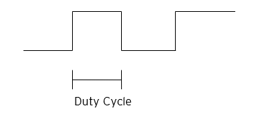
-
Frequency - The Frequency is a 32-bit value indicating the output frequency in Hertz. One over the frequency is the period.
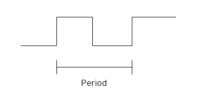
At controller power-up or during a download, the PWM output is maintained at zero until both the Frequency and the Duty cycle are loaded with non-zero values. When the controller is placed in stop mode, the state of the PWM out- puts is dependent on the PWM State on Controller Stop configuration. This configuration allows for either hold-last- state or specific frequency and duty cycle counts. Specifying zero for either the period or duty causes the PWM out- put to remain low during stop mode.
HSC840 Output Wave form
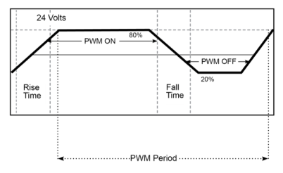
|
PWM Output Waveform Table |
|
|---|---|
| Rise Time | 150ns Max |
| Fall Time | 150ns Max |
| PWM Period | Frequency = 1 / Period |
HSC840 High Speed Counter Match
When any of Q1 to Q4 are configured for HSC Output operation, their output state is based on a comparison between the counter accumulator and match registers.
Stepper Function
The HSC840 supports four stepper functions, one on each high-speed output .
The Stepper requires five parameters (%AQs) to be set for operation. These parameters may be set at run-time but are ‘latched’ when the stepper is commanded to start:
|
Parameters |
Description |
|---|---|
| Start Frequency (Pulses per second) |
|
| Run Frequency (Pulses per second) |
|
| Acceleration Count |
|
| Run Count |
|
| Deceleration Count |
|
The Stepper provides two Boolean registers to provide stepper status:
| Ready/Done | A high indication on this register indicates the stepper sequence can be started (i.e. not currently busy) and also when the move is completed. |
| Error | A high indication on this register indicates that one of the analog parameters specified above is invalid or the stepper action was aborted before the operation was complete. This register is cleared on the next start command if the error was corrected. |
The stepper requires one discrete register to control the stepper action. Setting this register starts the stepper cycle. This register must remain set to complete the entire cycle. Clearing this register before the cycle is complete aborts the step sequence and sets the error bit.
NOTE: Setting the PLC mode to stop while the Stepper is in operation causes the Stepper output to immediately drop to zero and the current stepper count to be lost.
NOTE: The Stepper output level may cause damage or be incompatible with some motor drive inputs. Consult the drive documentation to determine if output level and type are compatible.
Return to the Top: OCS-I/O Modules
Stepper Examples
The following abbreviations are used in these examples:
-
Accelerates (Accel)
-
Decelerates (Decel)
Example 1
| Example 1 | Start Frequency | Run Frequency | Accel Count | Run Count | Decel Count |
|---|---|---|---|---|---|
| 10,000,000 steps control sequence | Set %AQ421 = 2500 (Hz) | Set %AQ422 = 5000 (Hz) | Set %AQ423-4 = 1,000,000 (Steps) | Set %AQ425-6 = 8,000,000 (Steps) | Set %AQ427-8 = 1,0000,000 (Steps) |
| When the start bit is energized, the example starts at 2.5kHz and ramps up to 5kHz during the first 1,000,000 steps. Then, it runs at 5kHz for the next 8,000,000 steps. Finally, during the last 1,000,000 steps it slows to a stop. | |||||
Example 2
| Example 2 | Start Frequency | Run Frequency | Accel Count | Run Count | Decel Count |
|---|---|---|---|---|---|
| 5,000,000 steps control sequence |
Set %AQ421 = 500 (Hz) |
Set %AQ422 = 1000 (Hz) |
Set %AQ423-4 = 2,000,000 (Steps) |
Set %AQ425-6 = 2,000,000 (Steps) |
Set %AQ427-8 = 1,000,000 (Steps) |
| When the start bit is energized, the example starts at 0.5 kHz and ramps up to 1 kHz during the first 2,000,000 steps. Then, it runs at 1 kHz for the next 2,000,000 steps. Finally, during the last 1,000,000 steps it slows to a stop. | |||||
Example 3
| Example 3 | Start Frequency | Run Frequency | Accel Count | Run Count | Decel Count |
|---|---|---|---|---|---|
| 6,000,000 steps control sequence |
Set %AQ421 = 50 (Hz) |
Set %AQ422 = 250 (Hz) |
Set %AQ423-4 = 150,000 (Steps) |
Set %AQ425-6 = 5,500,000 (Steps) |
Set %AQ427-8 = 350,000 (Steps) |
| When the start bit is energized, the following example starts at 50Hz and ramps up to 250Hz during the first 150,000 steps. Then, it runs at 250Hz for the next 5,500,000 steps. During the last 350,000 steps it slows to a stop. | |||||
NOTE: Prior to the start of a move, the Ready/Done bit for that channel must be ON (%I1617 or %I1619 for channel 1 and 2 respectfully). The Ready/Done bit will turn OFF during the move, and then back ON once the move is completed.
NOTE: The pulse generation hardware on the OCS can generate any frequency that can be evenly divided into 10MHz (10,000,000Hz) under the maximum recommended frequencies for each model. This results in a very smooth operation at lower frequencies, with a progressively choppier operation at higher frequencies, as the units reach their maximum recommended frequency.
PWM Examples
Example 1
| Example 1 | Duty Cycle | Frequency |
|---|---|---|
| To get a 50% Duty Cycle @ 10kHz waveform on PWM1: | Set %AQ421-422 = 16,000 | Set %AQ423-424 = 10,000 |
Example 2
| Example 2 | Duty Cycle | Frequency |
|---|---|---|
| To get a 50% Duty Cycle on PW1 and 90 % Duty Cycle on PWM2 @ 1kHz waveform: |
Set %AQ421-422 = 16,000 |
Set %AQ423-424 = 1,000 |
|
Set %AQ431-432 = 28,800 (duty cycle (32000 * 0.9)) |
Set %AQ433-434 = 1,000 |
Example 3
| Example 3 | Duty Cycle | Frequency |
|---|---|---|
| To turn PWM 1 output ON all the time | Set %AQ421-422 = 32,000 | Set %AQ423-424 = Any Value |
Example 4
| Example 4 | Duty Cycle | Frequency |
|---|---|---|
| To turn PWM 1 output OFF all the time | Set %AQ421-422 = 0 | Set %AQ423-424 = Any Value |
Return to the Top: OCS-I/O Modules
HSC I/O Filtering
This feature is used to enable digital Filter for HSC Inputs. Selecting Digital In/HSC configuration opens the following dialog wherein HSC I/O Filtering is available.
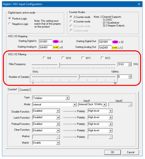
Input signal is filtered based on the filter frequency and Number of samples selected. User has to select Filter Frequency and Number of Samples based on the frequency of the Input signal.
-
Filter Frequency: To set the filter, choose a value that is: 4*Number of Samples*Expected Max Hz on the high-speed inputs.
-
Number of Samples: The input must be stable for this many samples before the HSC accumulator
A register/variable used to gather or accumulate a total of time, counts, items, or events. is affected by any change.
The state (high or low) of the high-speed input is sampled with every rising input edge of the filter frequency. The rising edges of the filter frequency are totaled in a sample counter, and when that total equals the number of samples configured, the sample counter is reset. If the high-speed input state did not change by the time of the sample counter reset, that state, high or low, is passed on to the high-speed accumulator. If the high-speed input state changes during the sample counting, the sample counter is reset to zero and the process starts over.
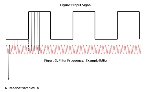
If user selects filter frequency as 1MHz and Number of samples as 4, then Input signal is sampled for 4 samples and if the signal is stable for 4 samples i.e. 4μs then the signal is passed to Accumulator![]() A register/variable used to gather or accumulate a total of time, counts, items, or events.. If the Input state is changed in between the sampling counts, then the count is reset, and the Input state is again checked for given number of samples.
A register/variable used to gather or accumulate a total of time, counts, items, or events.. If the Input state is changed in between the sampling counts, then the count is reset, and the Input state is again checked for given number of samples.
Refer to Dotted lines in the Figure 2, after 2 samples the state of input signal changes to 1, so the counter is again started to count 4 samples, to pass the signal to accumulator.
There will be a delay in passing the input signal to accumulator since we are filtering the Input signal and the delay is based on the selected filter frequency and Number of samples. In the above example filter frequency is 1MHZ (1μs) and number of samples: 4, so the minimum delay in input signal will be 4μs.
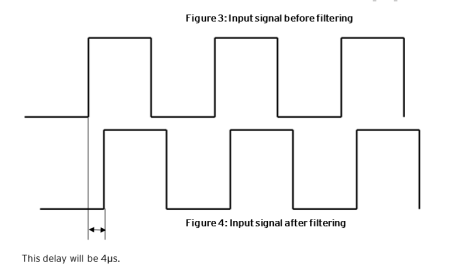
Return to the Top: OCS-I/O Modules
HSC840 Input Configurations:
For additional information, see High Speed Counter Terms, Defaults, and Definitions
-
Active Modes: Digital Input supports both Positive logic and Negative logic modes for 24V, 12V, 5V and 0V (Zero Crossing) voltage ranges.
-
Update Method:Digital Input supports update on change of state and updates periodically (10mS to 255 S).
-
HSC I/O Filtering: This feature is used to enable digital Filter for HSC Inputs to prevent false transition caused by spurious signals.
-
Sample Frequency: Set the Sample frequency to filter it.
-
Consecutive Samples: Set the number of samples, so the input must be stable for this many samples before the HSC accumulator is affected by any change.
-
Counter Configurations:
High-Speed Input supports the following modes:
-
Totalizer
-
Period Measurement
-
Frequency Counter
-
Pulse Width Measurement
-
Quadrature
-
-
High-speed input on the OCS contains optional functions as below and can be disabled or set to an internal pre-assigned register or to any external inputs.
-
Disable
-
Latch
-
Preload
-
Clear
-
Marker
-
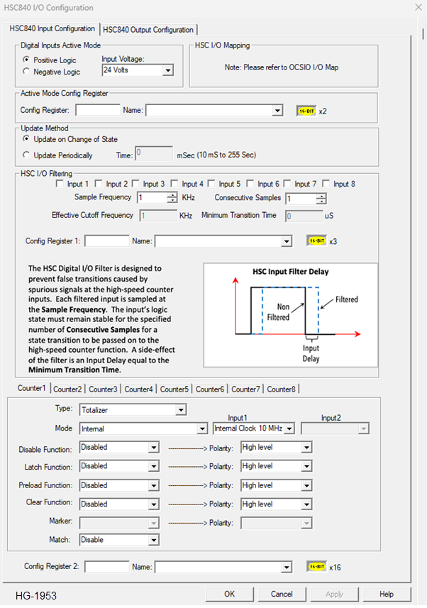
Return to the Top: OCS-I/O Modules
HSC840 Output Configurations:
High-Speed output supports the following modes.
-
Normal - Digital Output
-
PWM - Pulse Width Modulation
-
HSC Output - High Speed Counter Output
-
Stepper
-
PTO - Pulse Train Output
PWM Halt State Configuration
-
Duty Cycle: Set PWM output default duty cycle when the controller is in idle mode or the module is not in communication with the controller.
-
Frequency: Set PWM output default duty cycle when the controller is idle mode or the module is not in communication with the controller.
-
Hold state: Set this option to hold last state when the controller is idle mode or the module is not in communication with the controller
Return to the Top: OCS-I/O Modules
Normal Output Halt State Configuration:
Normal Digital Output can be set to On / Off / Hold when the controller is in idle mode or the module is not in communication with the controller.
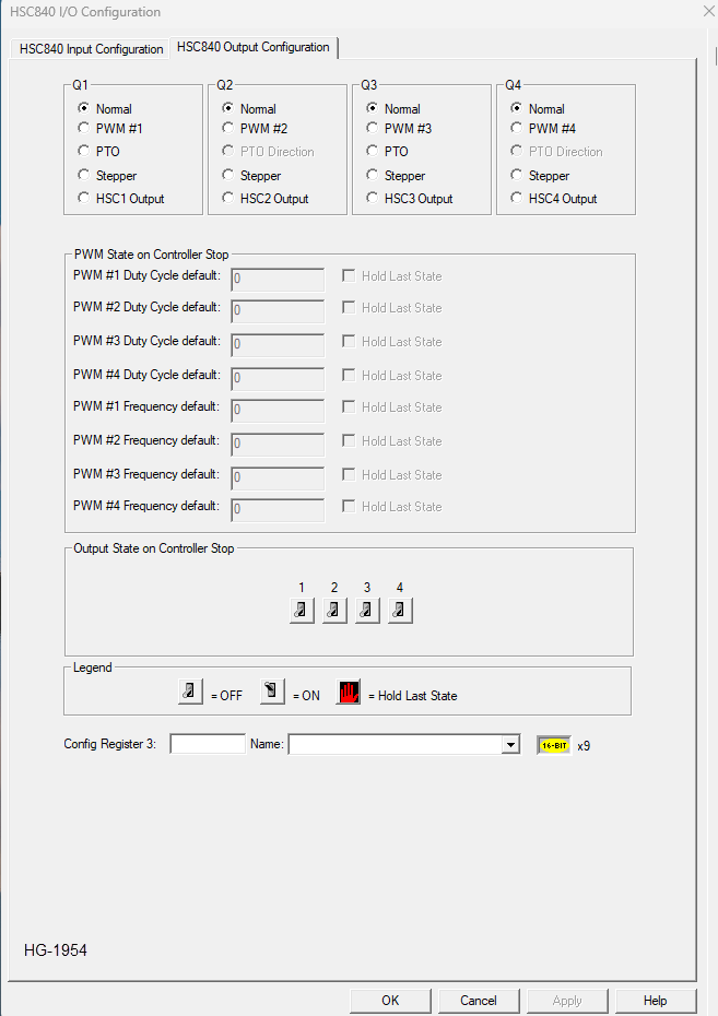
Return to the Top: OCS-I/O Modules
Register Mapping Details
On the Hardware Configuration screen, select the controller to be configured and then select Config. Or, if adding a controller, select Add.
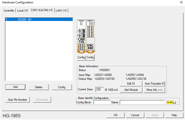
To view the I/O configured for a controller, on the Hardware Configuration screen, select the controller to be configured and then select Edit I/O or More Info.
Return to the Top: OCS-I/O Modules
Mixed Digital and Analog Module
MIX105 supports 4 - Digital Inputs, 4- Digital Outputs, 4- Analog Inputs (0-20/4-20 configurable) and 2-Analog Outputs (0-20/4-20 configurable).
Analog Input Settings
-
Filter Constant: Analog Inputs can be filtered Digitally with this Filter constant values. Valid filter values are 0 to 7.
-
Data Type: Select the input Data Type as 0-20 mA/ 4-20mA. Each analog input channel can be Disabled by selecting option” Disable” in the dropdown menu.
-
Data Range: Select the data range from the dropdown for the input. Analog input is scaled based on the Data type and Data range selected; and reflected in the configured register.
Data Range Input Type Data Range 0-20mA 0~4000, -2000~2000,0~1000,0~2000,0~32000 4-20mA 0~4000, -2000~2000, 0~1000, 400~2000,0~32000
-
Analog Input type, Data Range, Filter values can be selected through Register. Configure register in this field and user must move predefined values to the register to select the required input type, range and filter.
Digital Input Settings
-
Filter: Select the filter settings, for digital input modules. The changes in input state less than this setting are not reflected in the configured register.
-
Update Method:An I/O Module with digital inputs can be configured to update its digital input data either on change of state or periodically. The update period is programmable from 10 mS to 255 Seconds. If the update method is disabled, then Digital inputs will work based on periodic time configuration.
-
Digital Input Active Mode: Select the mode for Digital Input signal as either positive or Negative Logic.
-
Digital Output on Controller Stop: Digital outputs normally turn off if communication is lost with the Host Controller or if the Host Controller goes into IDLE mode. However, digital outputs can optionally be configured to hold last state or Turn ON instead.
-
Input Update Method: An I/O Module with analog inputs always updates its analog input data periodically. The update period is programmable from 10 mS to 255 Seconds.
Analog Output Settings
-
Data Type: Select the Analog Output type as 0-20ma or 4-20ma from the dropdown list.
-
Data Range: Select the data range for the analog output from the dropdown list. The analog output will be scaled according to the data in the configured register, selected data type and data range. Each analog Output channel can be Disabled by selecting option” Disable” in the dropdown.
Data Range Input Type Data Range 0-20mA 0~4000, -2000~2000, 0~1000, 0~2000, 0~32000 4-20mA 0~4000, -2000~2000, 0~1000, 400~2000,0~32000 -
Halt State: Each Analog output can be configured to either hold its current value or go to minimum, Average or maximum value, if communication is lost with the Host Controller or if the Host Controller goes into IDLE mode.
-
Analog Output type, Data Range, halt state values can be selected through Register. Configure register in this field and user must move predefined values to the register to select the required output type, range and halt state.
Return to the Top: OCS-I/O Modules
Stepper Status Boolean Registers
The Stepper provides two Boolean Registers to provide Stepper status.
| Status | Description |
| Read/Done | A high indication on this register indicates the Stepper sequence can be started (i.e., not currently busy), also when the move is completed. |
| Error | A high indication on this register indicates that one of the analog parameters specified is invalid or the Stepper action was aborted before the operation was complete. This register is cleared on the next start command if the error was corrected. |
The Stepper requires one discrete register to control the Stepper action. Setting this register starts the Stepper Cycle. This register must remain set to complete the entire cycle. Clearing this register before the cycle is complete aborts the step sequence and sets the error bit.
Note: Setting the PLC model to stop while the Stepper is in operation causes the Stepper output to immediately drop to zero and the current Stepper count to be lost.
Note: The Stepper output level may cause damage or be incompatible with some motor drive inputs. Consult the drive documentation to determine if the output level and type are comparative.
Return to the Top: OCS-I/O Modules
PTO Function
The HSC840 supports PTO (Pulse Train Output) output in Q1 and Q3, whereas Q2 and Q4 support PTO direction.
The PTO requires five parameters ( s) to be set for operation. These parameters may be set at run-time but are ‘latched’ when the stepper is commanded to start:
| Start Frequency
(pulses per second) |
Sets the frequency for the first cycle during the acceleration phase and the frequency of the last cycle during the deceleration phase. When an acceleration or deceleration count is specified, the Start Frequency must be greater than 0 and must not exceed the run frequency or an error is generated. |
| Run Frequency (pulses per second) |
Sets the frequency for the last cycle during the acceleration phase, the consistent frequency during the run phase, and the frequency of the first cycle during the deceleration mode. The Run Frequency must be greater than 0 and must not exceed 5000Hz (standard). |
| Acceleration Time | Sets the time(ms) required to linearly increase the frequency from Start Frequency to Run Frequency. Setting this value to zero disables the acceleration phase. |
| Pulse Count | Sets the total number of output pulses generated during the entire motion, including acceleration, constant speed, and deceleration phases. This parameter determines the total movement. |
| Deceleration Time | Sets the time(ms) required to linearly decrease the frequency from Run Frequency back to Start Frequency. Setting this value to zero disables the deceleration phase. |
Return to the Top: OCS-I/O Modules
The PTO provides two Stepper Status Boolean Registers registers to provide status.
| Status | Description |
| Read/Done | A high indication on this register indicates the Stepper sequence can be started (i.e., not currently busy), also when the move is completed. |
| Error | A high indication on this register indicates that one of the analog parameters specified is invalid or the Stepper action was aborted before the operation was complete. This register is cleared on the next start command if the error was corrected. |
-
The PTO function requires one discrete register to control the action of Q1 and Q3 channel. Setting this register starts the cycle and this register must remain set to complete the entire cycle. Clearing this register before the cycle is complete aborts the step sequence and sets the error bit.
-
The PTO function requires one discrete register to control the direction (Q2 and Q4). Setting this register is reverse direction and resetting the register is forward direction.
Note: Setting the PLC model to stop while the Stepper is in operation causes the Stepper output to immediately drop to zero and the current Stepper count to be lost.
Note: The Stepper output level may cause damage or be incompatible with some motor drive inputs. Consult the drive documentation to determine if the output level and type are comparative.
Note: Two HSC840 modules can be connected on the CScan network, using multiple bases or a single base configuration. When multiple HSC840 modules are added to the network, the CScan network traffic (%SR187) should be continuously monitored. If the network traffic (%SR187) exceeds 80%, it is recommended to change the update method to periodic to reduce communication load and ensure stable operation
Return to the Top: OCS-I/O Modules
MIX105 Dynamic I/O Configuration
Analog Input
AI Filter Constants - % R500
MIX105 Module AI channel Filter Constant Values 0 to 7 which is common for all 4 channels.
AI Data type- %R501
MIX105 Analog Input uses two consecutive 16-Bit registers for configuration, and each register has the following description. As an example, if %R801 is configured for Analog Inputs.
| Data Type | Value | ||
| 0-20mA | 1 | ||
| 4-20mA | 2 | ||
| Disable | 14 |
AI Data type- %R502
|
Range: 0-20mA |
Range: 4-20mA |
Value |
|---|---|---|
| 0~4000 | 0~4000 | 0 |
| -2000~2000 | -2000~2000 | 1 |
| 0~1000 | 0~1000 | 2 |
| 0~2000 | Reserved | 3 |
| Reserved | 400~2000 | 4 |
| 0~32000 | 0~32000 | 5 |
| Reserved | Reserved | 6 |
| Reserved | Reserved | 7 |
| Reserved | Reserved | 8 |
Analog Output: Description
Analog Output uses three consecutive 16-Bit registers for configuration, and each register has the following description: As an example, if %R505 is configured for Analog Output channel.
Analog Output Data Type: %R505
|
Data Type |
Value |
|---|---|
| 0-20mA | 1 |
| 4-20mA | 2 |
| Disable | 14 |
Analog Output Data Range: %R506
|
Range: 0-20mA |
Range: 4-20mA |
Value |
|---|---|---|
| 0~4000 | 0~4000 | 0 |
| -2000~2000 | -2000~2000 | 1 |
| 0~1000 | 0~1000 | 2 |
| 0~2000 | Reserved | 3 |
| Reserved | 400~2000 | 4 |
| 0~32000 | 0~32000 | 5 |
Analog Output Halt State: %R507
|
Halt State |
Value |
|---|---|
| Current | 0 |
| Minimum | 1 |
| Maximum | 2 |
| Average | 3 |
Return to the Top: OCS-I/O Modules
NTC800 Dynamic I/O Configuration
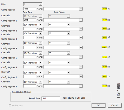
AI Filter Constants - %R100
NTC800 Module AI channel Filter Constant Values 0 to 7 which is common for all 8 channels
Channels Configuration
AI Data Type %R200
| Data Type | Value | ||
| 10K Thermistor | 15 | ||
| Disable | 14 |
AI Data Range %R202
|
Thermistor |
Value |
|---|---|
| Reserved | 0 |
| Reserved | 1 |
| Reserved | 2 |
| Reserved | 3 |
| Reserved | 4 |
| Reserved | 5 |
| Reserved | 6 |
| °C | 7 |
| °F | 8 |